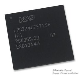
MCU 16-bit/32-bit LPC3000 ARM926EJ-S RISC ROMLess 1.2V/1.8V/2.5V/3.3V 296-Pin TF-BGA Tray, LPC3240FET296/01,5, NXP

The LPC3240 operates at CPU frequencies of up to 266 MHz. The NXP implementation uses an ARM926EJ-S CPU core with a Harvard architectur, 5-stage pipeline, and an integral Memory Management Unit (MMU). The LPC3240 also includes 256 kB of on-chip static RAM, a NAND flash interface, an Ethernet MAC, and an external bus interface that supports SDR and DDR SDRAM, as well as static devices. In addition, the LPC3240 includes a USB 2.0 full-speed interface, seven UARTs, two I2C-bus interfaces, two SPI/SSP ports, two I2S-bus interfaces, two single output PWMs, a motor control PWM, six general purpose timers with capture inputs and compare outputs, a Secure Digital (SD) interface, and a 10-bit Analog-to-Digital Converter (ADC) with a touch screen sense option.

  • ARM926EJS processor, running at CPU clock speeds up to 266 MHz
  • Vector Floating Point (VFP) coprocessor
  • 32 kB instruction cache and a 32 kB data cache
  • Up to 256 kB of Internal SRAM (IRAM)
  • Selectable boot-up from various external devices
  • Multi-layer AHB system that provides a separate bus for each AHB master
  • External memory controller for DDR and SDR SDRAM as well as for static devices
  • Two NAND flash controllers
  • Master Interrupt Controller (MIC) and two Slave Interrupt Controllers (SIC)
  • Eight channel General Purpose DMA (GPDMA) controller on the AHB
  • 10/100 Ethernet MAC with dedicated DMA Controller
  • USB interface supporting either device, host (OHCI compliant), or On-The-Go
  • Four standard UARTs with fractional baud rate generation
  • Three additional high-speed UARTs intended for on-board communications
  • Two SPI controllers
  • Two SSP controllers
  • Two I2C-bus interfaces with standard open-drain pins
  • Two I2S-bus interfaces, each with separate input and output channels
  • Secure Digital (SD) memory card interface
  • General Purpose (GP) input, output, and I/O pins
  • 10 bit, 400 kHz Analog-to-Digital Converter (ADC)
  • Real-Time Clock (RTC) with separate power pin and dedicated 32 kHz oscillator
  • 32-bit general purpose high-speed timer with a 16-bit pre-scaler
  • Six enhanced timer/counters
  • 32-bit millisecond timer driven from the RTC clock
  • WatchDog timer clocked by the peripheral clock
  • Two single-output PWM blocks
  • Motor control PWM
  • Keyboard scanner function allows automatic scanning of an up to 8 x 8 key matrix
  • Up to 18 external interrupts
  • Standard ARM test/debug interface for compatibility with existing tools
  • Emulation Trace Buffer (ETB) with 2048 x 24 bit RAM allows trace via JTAG
  • Stop mode saves power
  • On-chip crystal oscillator
  • An on-chip PLL allows CPU operation up to the maximum CPU rate
  • Boundary scan for simplified board testing
Характеристики

Product_dimensions

15.1 x 15.1 x 0.8 mm

Eccn

EAR99

Schedule_b

8542310000

Ram_size

256 KB

Program_memory_type

ROMLess

Pin_count

296

Supplier_package

TFBGA

Operating_temperature

-40 to 85 °C

Operating_supply_voltage

1.2, 1.8, 2.5, 3.3 V

Specifications

https://4donline.ihs.com/images/VipMasterIC/IC/PHGL/PHGL-S-A0001382872/PHGL-S-A0001382872-1.pdf?hkey=52A5661711E402568146F3353EA87419

Watchdog

1

On_chip_adc

8-chx10-bit

Number_of_timers

6

Htsn

8542310001

Screening_level

Industrial

Data_bus_width

16, 32 Bit

Device_core

ARM926EJ-S

Country_of_origin

Taiwan

Бренд

Instruction_set_architecture

RISC

Тип интерфейса

Ethernet/I2C/I2S/SPI/UART/USB

Number_of_programmable_i_os

51

Max_speed

266 MHz

Msl_level

3

Mounting

Surface Mount

Min_operating_supply_voltage

0.9, 1.1, 1.31, 1.7, 2.3, 2.7 V

Max_processing_temp

250 °C

Max_power_dissipation

1120 mW

Max_operating_supply_voltage

1.39, 1.95, 2.7, 3.6 V

Lead_finish

Tin/Silver/Copper

Артикул: LPC3240FET296/01,5

Описание

The LPC3240 operates at CPU frequencies of up to 266 MHz. The NXP implementation uses an ARM926EJ-S CPU core with a Harvard architectur, 5-stage pipeline, and an integral Memory Management Unit (MMU). The LPC3240 also includes 256 kB of on-chip static RAM, a NAND flash interface, an Ethernet MAC, and an external bus interface that supports SDR and DDR SDRAM, as well as static devices. In addition, the LPC3240 includes a USB 2.0 full-speed interface, seven UARTs, two I2C-bus interfaces, two SPI/SSP ports, two I2S-bus interfaces, two single output PWMs, a motor control PWM, six general purpose timers with capture inputs and compare outputs, a Secure Digital (SD) interface, and a 10-bit Analog-to-Digital Converter (ADC) with a touch screen sense option.

  • ARM926EJS processor, running at CPU clock speeds up to 266 MHz
  • Vector Floating Point (VFP) coprocessor
  • 32 kB instruction cache and a 32 kB data cache
  • Up to 256 kB of Internal SRAM (IRAM)
  • Selectable boot-up from various external devices
  • Multi-layer AHB system that provides a separate bus for each AHB master
  • External memory controller for DDR and SDR SDRAM as well as for static devices
  • Two NAND flash controllers
  • Master Interrupt Controller (MIC) and two Slave Interrupt Controllers (SIC)
  • Eight channel General Purpose DMA (GPDMA) controller on the AHB
  • 10/100 Ethernet MAC with dedicated DMA Controller
  • USB interface supporting either device, host (OHCI compliant), or On-The-Go
  • Four standard UARTs with fractional baud rate generation
  • Three additional high-speed UARTs intended for on-board communications
  • Two SPI controllers
  • Two SSP controllers
  • Two I2C-bus interfaces with standard open-drain pins
  • Two I2S-bus interfaces, each with separate input and output channels
  • Secure Digital (SD) memory card interface
  • General Purpose (GP) input, output, and I/O pins
  • 10 bit, 400 kHz Analog-to-Digital Converter (ADC)
  • Real-Time Clock (RTC) with separate power pin and dedicated 32 kHz oscillator
  • 32-bit general purpose high-speed timer with a 16-bit pre-scaler
  • Six enhanced timer/counters
  • 32-bit millisecond timer driven from the RTC clock
  • WatchDog timer clocked by the peripheral clock
  • Two single-output PWM blocks
  • Motor control PWM
  • Keyboard scanner function allows automatic scanning of an up to 8 x 8 key matrix
  • Up to 18 external interrupts
  • Standard ARM test/debug interface for compatibility with existing tools
  • Emulation Trace Buffer (ETB) with 2048 x 24 bit RAM allows trace via JTAG
  • Stop mode saves power
  • On-chip crystal oscillator
  • An on-chip PLL allows CPU operation up to the maximum CPU rate
  • Boundary scan for simplified board testing
Детали

Product_dimensions

15.1 x 15.1 x 0.8 mm

Eccn

EAR99

Schedule_b

8542310000

Ram_size

256 KB

Program_memory_type

ROMLess

Pin_count

296

Supplier_package

TFBGA

Operating_temperature

-40 to 85 °C

Operating_supply_voltage

1.2, 1.8, 2.5, 3.3 V

Specifications

https://4donline.ihs.com/images/VipMasterIC/IC/PHGL/PHGL-S-A0001382872/PHGL-S-A0001382872-1.pdf?hkey=52A5661711E402568146F3353EA87419

Watchdog

1

On_chip_adc

8-chx10-bit

Number_of_timers

6

Htsn

8542310001

Screening_level

Industrial

Data_bus_width

16, 32 Bit

Device_core

ARM926EJ-S

Country_of_origin

Taiwan

Бренд

Instruction_set_architecture

RISC

Тип интерфейса

Ethernet/I2C/I2S/SPI/UART/USB

Number_of_programmable_i_os

51

Max_speed

266 MHz

Msl_level

3

Mounting

Surface Mount

Min_operating_supply_voltage

0.9, 1.1, 1.31, 1.7, 2.3, 2.7 V

Max_processing_temp

250 °C

Max_power_dissipation

1120 mW

Max_operating_supply_voltage

1.39, 1.95, 2.7, 3.6 V

Lead_finish

Tin/Silver/Copper