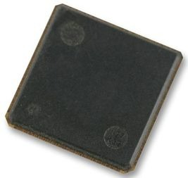
MCU 32-bit LPC1700 ARM Cortex M3 RISC 512KB Flash 3.3V 100-Pin TF-BGA Tray, LPC1768FET100,551, NXP

The LPC1769/68/67/66/65/64/63 are ARM Cortex-M3 based microcontrollers for embedded applications featuring a high level of integration and low power consumption. The ARM Cortex-M3 is a next generation core that offers system enhancements such as enhanced debug features and a higher level of support block integration. The LPC1768/67/66/65/64/63 operate at CPU frequencies of up to 100 MHz. The LPC1769 operates at CPU frequencies of up to 120 MHz. The ARM Cortex-M3 CPU incorporates a 3-stage pipeline and uses a Harvard architecture with separate local instruction and data buses as well as a third bus for peripherals. The ARM Cortex-M3 CPU also includes an internal prefetch unit that supports speculative branching. The peripheral complement of the LPC1769/68/67/66/65/64/63 includes up to 512 kB of flash memory, up to 64 kB of data memory, Ethernet MAC, USB Device/Host/OTG interface, 8-channel general purpose DMA controller, 4 UARTs, 2 CAN channels, 2 SSP controllers, SPI interface, 3 I2C-bus interfaces, 2-input plus 2-output I2S-bus interface, 8-channel 12-bit ADC, 10-bit DAC, motor control PWM, Quadrature Encoder interface, four general purpose timers, 6-output general purpose PWM, ultra-low power Real-Time Clock (RTC) with separate battery supply, and up to 70 general purpose I/O pins.

  • ARM Cortex-M3 processor, running at frequencies of up to 100 MHz (LPC1768/67/66/65/64/63) or of up to 120 MHz (LPC1769). A Memory Protection Unit (MPU) supporting eight regions is included.
  • ARM Cortex-M3 built-in Nested Vectored Interrupt Controller (NVIC).
  • Up to 512 kB on-chip flash programming memory. Enhanced flash memory accelerator enables high-speed 120 MHz operation with zero wait states.
  • In-System Programming (ISP) and In-Application Programming (IAP) via on-chip bootloader software.
  • On-chip SRAM includes:
    • 32/16 kB of SRAM on the CPU with local code/data bus for high-performance CPU access.
    • Two/one 16 kB SRAM blocks with separate access paths for higher throughput. These SRAM blocks may be used for Ethernet, USB, and DMA memory, as well as for general purpose CPU instruction and data storage.
  • Eight channel General Purpose DMA controller (GPDMA) on the AHB multilayer matrix that can be used with SSP, I2S-bus, UART, Analog-to-Digital and Digital-to-Analog converter peripherals, timer match signals, and for memory-to-memory transfers.
  • Multilayer AHB matrix interconnect provides a separate bus for each AHB master. AHB masters include the CPU, General Purpose DMA controller, Ethernet MAC, and the USB interface. This interconnect provides communication with no arbitration delays.
Характеристики

Product_dimensions

9.1 x 9.1 x 0.8 mm

Eccn

EAR99

Schedule_b

8542310000

Ram_size

64 KB

Program_memory_type

Flash

Program_memory_size

512 Kb

Pin_count

100

Supplier_package

TFBGA

Operating_temperature

-40 to 85 °C

Operating_supply_voltage

3.3 V

Specifications

https://4donline.ihs.com/images/VipMasterIC/IC/PHGL/PHGLS29828/PHGLS29828-1.pdf?hkey=52A5661711E402568146F3353EA87419

Watchdog

1

On_chip_adc

8-chx12-bit

Number_of_timers

4

Htsn

8542310001

Special_features

CAN Controller

Data_bus_width

32 Bit

Device_core

ARM Cortex M3

Country_of_origin

Taiwan

Бренд

Instruction_set_architecture

RISC

Тип интерфейса

CAN/Ethernet/I2C/I2S/SPI/SSP/UART/USB

Number_of_programmable_i_os

70

Max_speed

100 MHz

Msl_level

3

Mounting

Surface Mount

Min_operating_supply_voltage

2.4 V

Max_processing_temp

260 °C

Max_power_dissipation

1500 mW

Max_operating_supply_voltage

3.6 V

Max_expanded_memory_size

1 GB

Lead_finish

Tin/Silver/Copper

Артикул: LPC1768FET100,551

Описание

The LPC1769/68/67/66/65/64/63 are ARM Cortex-M3 based microcontrollers for embedded applications featuring a high level of integration and low power consumption. The ARM Cortex-M3 is a next generation core that offers system enhancements such as enhanced debug features and a higher level of support block integration. The LPC1768/67/66/65/64/63 operate at CPU frequencies of up to 100 MHz. The LPC1769 operates at CPU frequencies of up to 120 MHz. The ARM Cortex-M3 CPU incorporates a 3-stage pipeline and uses a Harvard architecture with separate local instruction and data buses as well as a third bus for peripherals. The ARM Cortex-M3 CPU also includes an internal prefetch unit that supports speculative branching. The peripheral complement of the LPC1769/68/67/66/65/64/63 includes up to 512 kB of flash memory, up to 64 kB of data memory, Ethernet MAC, USB Device/Host/OTG interface, 8-channel general purpose DMA controller, 4 UARTs, 2 CAN channels, 2 SSP controllers, SPI interface, 3 I2C-bus interfaces, 2-input plus 2-output I2S-bus interface, 8-channel 12-bit ADC, 10-bit DAC, motor control PWM, Quadrature Encoder interface, four general purpose timers, 6-output general purpose PWM, ultra-low power Real-Time Clock (RTC) with separate battery supply, and up to 70 general purpose I/O pins.

  • ARM Cortex-M3 processor, running at frequencies of up to 100 MHz (LPC1768/67/66/65/64/63) or of up to 120 MHz (LPC1769). A Memory Protection Unit (MPU) supporting eight regions is included.
  • ARM Cortex-M3 built-in Nested Vectored Interrupt Controller (NVIC).
  • Up to 512 kB on-chip flash programming memory. Enhanced flash memory accelerator enables high-speed 120 MHz operation with zero wait states.
  • In-System Programming (ISP) and In-Application Programming (IAP) via on-chip bootloader software.
  • On-chip SRAM includes:
    • 32/16 kB of SRAM on the CPU with local code/data bus for high-performance CPU access.
    • Two/one 16 kB SRAM blocks with separate access paths for higher throughput. These SRAM blocks may be used for Ethernet, USB, and DMA memory, as well as for general purpose CPU instruction and data storage.
  • Eight channel General Purpose DMA controller (GPDMA) on the AHB multilayer matrix that can be used with SSP, I2S-bus, UART, Analog-to-Digital and Digital-to-Analog converter peripherals, timer match signals, and for memory-to-memory transfers.
  • Multilayer AHB matrix interconnect provides a separate bus for each AHB master. AHB masters include the CPU, General Purpose DMA controller, Ethernet MAC, and the USB interface. This interconnect provides communication with no arbitration delays.

Детали

Product_dimensions

9.1 x 9.1 x 0.8 mm

Eccn

EAR99

Schedule_b

8542310000

Ram_size

64 KB

Program_memory_type

Flash

Program_memory_size

512 Kb

Pin_count

100

Supplier_package

TFBGA

Operating_temperature

-40 to 85 °C

Operating_supply_voltage

3.3 V

Specifications

https://4donline.ihs.com/images/VipMasterIC/IC/PHGL/PHGLS29828/PHGLS29828-1.pdf?hkey=52A5661711E402568146F3353EA87419

Watchdog

1

On_chip_adc

8-chx12-bit

Number_of_timers

4

Htsn

8542310001

Special_features

CAN Controller

Data_bus_width

32 Bit

Device_core

ARM Cortex M3

Country_of_origin

Taiwan

Бренд

Instruction_set_architecture

RISC

Тип интерфейса

CAN/Ethernet/I2C/I2S/SPI/SSP/UART/USB

Number_of_programmable_i_os

70

Max_speed

100 MHz

Msl_level

3

Mounting

Surface Mount

Min_operating_supply_voltage

2.4 V

Max_processing_temp

260 °C

Max_power_dissipation

1500 mW

Max_operating_supply_voltage

3.6 V

Max_expanded_memory_size

1 GB

Lead_finish

Tin/Silver/Copper