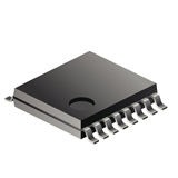
MCU 32-Bit LPC800 ARM Cortex M0+ RISC 8KB Flash 3.3V 16-Pin TSSOP, LPC811M001JDH16FP, NXP

The LPC811M001FDH16 is an ARM Cortex-M0+ based, low-cost 32-bit MCU operating at CPU frequencies of up to 30 MHz. The peripheral complement of the LPC811M001FDH16 includes 8 kB of flash memory, 2 kB of data memory, CRC engine, one I²C-bus interface, two USARTs, one SPI interface, multi-rate timer, self wakeup timer, state-configurable timer, one comparator, function-configurable I/O ports through a switch matrix, an input pattern match engine and 14 general purpose I/O pins.

  • System:
    • ARM Cortex-M0+ processor, running at frequencies of up to 30 MHz withsingle-cycle multiplier and fast single-cycle I/O port
    • ARM Cortex-M0+ built-in Nested Vectored Interrupt Controller (NVIC)
    • System tick timer
    • Serial Wire Debug (SWD) and JTAG boundary scan modes supported
    • Micro Trace Buffer (MTB) supported
  • Memory:
    • 8 kB on-chip flash programming memory
    • 2 kB SRAM
  • Boot ROM API support:
    • Boot loader
    • USART drivers
    • I²C drivers
    • Power profiles
    • Flash In-Application Programming (IAP) and In-System Programming (ISP)
  • Digital peripherals:
    • High-speed GPIO interface connected to the ARM Cortex-M0+ IO bus with 14 General Purpose I/O (GPIO) pins with configurable pull-up/pull-down resistors
    • GPIO interrupt generation capability with boolean pattern-matching feature on eightGPIO inputs
    • Switch matrix for flexible configuration of each I/O pin function
    • State Configurable Timer (SCT) with input and output functions (including captureand match) assigned to pins through the switch matrix
    • Multiple-channel multi-rate timer for repetitive interrupt generation at up to fourprogrammable, fixed rates
    • Self Wake-up Timer (WKT) clocked from either the IRC or a low-power,low-frequency internal oscillator
    • CRC engine
    • Windowed Watchdog timer
  • Analog peripherals:
    • Comparator with external voltage reference with pin functions assigned or enabledthrough the switch matrix
  • Serial interfaces:
    • Two USART interfaces with pin functions assigned through the switch matrix
    • One SPI controller with pin functions assigned through the switch matrix
    • One I²C-bus interface with pin functions assigned through the switch matrix
  • Clock generation:
    • 12 MHz internal RC oscillator trimmed to 1 % accuracy that can optionally be usedas a system clock.
    • Crystal oscillator with an operating range of 1 MHz to 25 MHz
    • Programmable watchdog oscillator with a frequency range of 9.4 kHz to 2.3 MHz
    • 10 kHz low-power oscillator for the WKT
    • PLL allows CPU operation up to the maximum CPU rate without the need for ahigh-frequency crystal. May be run from the system oscillator, the external clockinput CLKIN, or the internal RC oscillator
    • Clock output function with divider that can reflect the crystal oscillator, the mainclock, the IRC, or the watchdog oscillator
  • Power control:
    • Integrated PMU (Power Management Unit) to minimize power consumption
    • Reduced power modes: Sleep mode, Deep-sleep mode, Power-down mode, andDeep power-down mode
    • Power-On Reset (POR)
    • Brownout detect
  • Unique device serial number for identification
  • Single power supply
  • Available as TSSOP16 package

Характеристики

Product_dimensions

5 x 4.4 x 0.95(Max)

Schedule_b

8542310000

Ram_size

2 KB

Program_memory_type

Flash

Program_memory_size

8 KB

Pin_count

16

Supplier_package

TSSOP

Operating_temperature

-40 to 105 °C

Operating_supply_voltage

3.3 V

Specifications

https://4donline.ihs.com/images/VipMasterIC/IC/PHGL/PHGL-S-A0001056910/PHGL-S-A0001056910-1.pdf?hkey=52A5661711E402568146F3353EA87419

Watchdog

1

Number_of_timers

4

Analog_comparators

1

Htsn

8542310001

Eccn

EAR99

Device_core

ARM Cortex M0+

Data_bus_width

32 Bit

Country_of_origin

China

Бренд

Instruction_set_architecture

RISC

Тип интерфейса

I2C/SPI/USART

Number_of_programmable_i_os

14

Max_speed

30 MHz

Msl_level

1

Mounting

Surface Mount

Min_operating_supply_voltage

1.8 V

Max_processing_temp

260 °C

Max_power_dissipation

1500 mW

Max_operating_supply_voltage

3.6 V

Lead_finish

Gold Over Nickel Palladium

Артикул: LPC811M001JDH16FP

Описание

The LPC811M001FDH16 is an ARM Cortex-M0+ based, low-cost 32-bit MCU operating at CPU frequencies of up to 30 MHz. The peripheral complement of the LPC811M001FDH16 includes 8 kB of flash memory, 2 kB of data memory, CRC engine, one I²C-bus interface, two USARTs, one SPI interface, multi-rate timer, self wakeup timer, state-configurable timer, one comparator, function-configurable I/O ports through a switch matrix, an input pattern match engine and 14 general purpose I/O pins.

  • System:
    • ARM Cortex-M0+ processor, running at frequencies of up to 30 MHz withsingle-cycle multiplier and fast single-cycle I/O port
    • ARM Cortex-M0+ built-in Nested Vectored Interrupt Controller (NVIC)
    • System tick timer
    • Serial Wire Debug (SWD) and JTAG boundary scan modes supported
    • Micro Trace Buffer (MTB) supported
  • Memory:
    • 8 kB on-chip flash programming memory
    • 2 kB SRAM
  • Boot ROM API support:
    • Boot loader
    • USART drivers
    • I²C drivers
    • Power profiles
    • Flash In-Application Programming (IAP) and In-System Programming (ISP)
  • Digital peripherals:
    • High-speed GPIO interface connected to the ARM Cortex-M0+ IO bus with 14 General Purpose I/O (GPIO) pins with configurable pull-up/pull-down resistors
    • GPIO interrupt generation capability with boolean pattern-matching feature on eightGPIO inputs
    • Switch matrix for flexible configuration of each I/O pin function
    • State Configurable Timer (SCT) with input and output functions (including captureand match) assigned to pins through the switch matrix
    • Multiple-channel multi-rate timer for repetitive interrupt generation at up to fourprogrammable, fixed rates
    • Self Wake-up Timer (WKT) clocked from either the IRC or a low-power,low-frequency internal oscillator
    • CRC engine
    • Windowed Watchdog timer
  • Analog peripherals:
    • Comparator with external voltage reference with pin functions assigned or enabledthrough the switch matrix
  • Serial interfaces:
    • Two USART interfaces with pin functions assigned through the switch matrix
    • One SPI controller with pin functions assigned through the switch matrix
    • One I²C-bus interface with pin functions assigned through the switch matrix
  • Clock generation:
    • 12 MHz internal RC oscillator trimmed to 1 % accuracy that can optionally be usedas a system clock.
    • Crystal oscillator with an operating range of 1 MHz to 25 MHz
    • Programmable watchdog oscillator with a frequency range of 9.4 kHz to 2.3 MHz
    • 10 kHz low-power oscillator for the WKT
    • PLL allows CPU operation up to the maximum CPU rate without the need for ahigh-frequency crystal. May be run from the system oscillator, the external clockinput CLKIN, or the internal RC oscillator
    • Clock output function with divider that can reflect the crystal oscillator, the mainclock, the IRC, or the watchdog oscillator
  • Power control:
    • Integrated PMU (Power Management Unit) to minimize power consumption
    • Reduced power modes: Sleep mode, Deep-sleep mode, Power-down mode, andDeep power-down mode
    • Power-On Reset (POR)
    • Brownout detect
  • Unique device serial number for identification
  • Single power supply
  • Available as TSSOP16 package

Детали

Product_dimensions

5 x 4.4 x 0.95(Max)

Schedule_b

8542310000

Ram_size

2 KB

Program_memory_type

Flash

Program_memory_size

8 KB

Pin_count

16

Supplier_package

TSSOP

Operating_temperature

-40 to 105 °C

Operating_supply_voltage

3.3 V

Specifications

https://4donline.ihs.com/images/VipMasterIC/IC/PHGL/PHGL-S-A0001056910/PHGL-S-A0001056910-1.pdf?hkey=52A5661711E402568146F3353EA87419

Watchdog

1

Number_of_timers

4

Analog_comparators

1

Htsn

8542310001

Eccn

EAR99

Device_core

ARM Cortex M0+

Data_bus_width

32 Bit

Country_of_origin

China

Бренд

Instruction_set_architecture

RISC

Тип интерфейса

I2C/SPI/USART

Number_of_programmable_i_os

14

Max_speed

30 MHz

Msl_level

1

Mounting

Surface Mount

Min_operating_supply_voltage

1.8 V

Max_processing_temp

260 °C

Max_power_dissipation

1500 mW

Max_operating_supply_voltage

3.6 V

Lead_finish

Gold Over Nickel Palladium