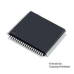
MCU 16-bit/32-bit TMS470 ARM7TDMI RISC 64KB Flash 1.8V/3.3V 80-Pin LQFP Tray, TMS470R1A64PNT, Texas Instruments

The TMS470R1A64 (2) device is a member of the Texas Instruments TMS470R1x family of general-purpose 16/32-bit reduced instruction set computer (RISC) microcontrollers. The A64 microcontroller offers high performance utilizing the high-speed ARM7TDMI 16/32-bit RISC central processing unit (CPU), resulting in a high instruction throughput while maintaining high code efficiency. The ARM7TDMI 16/32-bit RISC CPU views memory as a linear collection of bytes numbered upwards from 0. The TMS470R1A64 utilizes the big-endian format, where the most significant byte of a word is stored at the lowest numbered byte and the least significant byte at the highest numbered byte.High-end embedded control applications demand more performance from their controllers while maintaining low costs. The A64 RISC core architecture offers solutions to these performance and cost demands while maintaining low power consumption.The A64 memory includes general-purpose SRAM supporting single-cycle read/write accesses in byte, half-word, and word modes.The flash memory on the A64 device is a nonvolatile, electrically erasable and programmable memory implemented with a 32-bit-wide data bus interface. The flash operates with a system clock frequency of up to 24 MHz. In pipeline mode, the flash operates with a system clock frequency of up to 48 MHz.The A64 device has six communication interfaces: two SPIs, two SCIs, an SCC, and a C2SIa. The SPI provides a convenient method of serial interaction for high-speed communications between similar shift-register type devices. The SCI is a full-duplex, serial I/O interface intended for asynchronous communication between the CPU and other peripherals using the standard non-return-to-zero (NRZ) format. The SCC uses a serial, multimaster communication protocol that efficiently supports distributed real-time control with robust communication rates of up to 1 megabit per second (Mbps). The SCC is ideal for applications operating in noisy and harsh environments (e.g., industrial fields) that require reliable serial communication or multiplexed wiring. The C2SIa allows the A64 to transmit and receive messages on a class II network following an SAE J1850 (3) standard.

  • High-Performance Static CMOS Technology
  • TMS470R1x 16/32-Bit RISC Core (ARM7TDMI™)
    • 24-MHz System Clock (48-MHz Pipeline Mode)
    • Independent 16/32-Bit Instruction Set
    • Open Architecture With Third-Party Support
    • Built-In Debug Module
    • Big-Endian Format Utilized
  • Integrated Memory
    • 64K-Byte Program Flash
      • One Bank With Five Contiguous Sectors
      • Internal State Machine for Programming and Erase
    • 8K-Byte Static RAM (SRAM)
  • Operating Features
    • Core Supply Voltage (VCC): 1.71 V-2.06 V
    • I/O Supply Voltage (VCCIO): 3.0 V-3.6 V
    • Low-Power Modes: STANDBY and HALT
    • Extended Industrial Temperature Range
  • 470+ System Module
    • 32-Bit Address Space Decoding
    • Bus Supervision for Memory and Peripherals
    • Analog Watchdog (AWD) Timer
    • Real-Time Interrupt (RTI)
    • System Integrity and Failure Detection
  • Zero-Pin Phase-Locked Loop (ZPLL)-Based Clock Module With Prescaler
    • Multiply-by-4 or -8 Internal ZPLL Option
    • ZPLL Bypass Mode
  • Six Communication Interfaces:
    • Two Serial Peripheral Interfaces (SPIs)
      • 255 Programmable Baud Rates
    • Two Serial Communication Interfaces (SCIs)
      • 224 Selectable Baud Rates
      • Asynchronous/Isosynchronous Modes
    • Standard CAN Controller (SCC)
      • 16-Mailbox Capacity
      • Fully Compliant With CAN Protocol, Version 2.0B
    • Class II Serial Interface (C2SIa)
      • Two Selectable Data Rates
      • Normal Mode 10.4 Kbps and 4X Mode 41.6 Kbps
  • High-End Timer (HET)
    • 13 Programmable I/O Channels:
      • 12 High-Resolution Pins
      • 1 Standard-Resolution Pin
    • High-Resolution Share Feature (XOR)
    • HET RAM (64-Instruction Capacity)
  • 10-Bit Multi-Buffered ADC (MibADC) 8-Channel
    • 64-Word FIFO Buffer
    • Single- or Continuous-Conversion Modes
    • 1.55 µs Minimum Sample and Conversion Time
    • Calibration Mode and Self-Test Features
  • 6 External Interrupts
  • Flexible Interrupt Handling
  • 5 Dedicated General-Purpose I/O (GIO) Pins, 1 Input-Only GIO Pin, and 34 Additional Peripheral I/Os
  • External Clock Prescale (ECP) Module
    • Programmable Low-Frequency External Clock (CLK)
  • On-Chip Scan-Base Emulation Logic, IEEE Standard 1149.1(1) (JTAG) Test-Access Port
  • 80-Pin Plastic Low-Profile Quad Flatpack (PN Suffix)
  • Характеристики

    Product_dimensions

    12 x 12 x 1.4 mm

    Eccn

    3A991.A.2

    Ram_size

    8 KB

    Program_memory_type

    Flash

    Program_memory_size

    64 KB

    Pin_count

    80

    Supplier_package

    LQFP

    Operating_temperature

    -40 to 105 °C

    Operating_supply_voltage

    1.8, 3.3 V

    Specifications

    http://www.ti.com/general/docs/lit/getliterature.tsp?genericPartNumber=TMS470R1A64&&fileType=pdf

    On_chip_adc

    8-chx10-bit

    Number_of_timers

    1

    Htsn

    8542310001

    Schedule_b

    8542310000

    Data_bus_width

    16, 32 Bit

    Device_core

    ARM7TDMI

    Country_of_origin

    United States

    Бренд

    Instruction_set_architecture

    RISC

    Тип интерфейса

    SCI/SPI

    Number_of_programmable_i_os

    39

    Max_speed

    48 MHz

    Msl_level

    3

    Mounting

    Surface Mount

    Min_operating_supply_voltage

    1.71, 3 V

    Max_processing_temp

    260 °C

    Max_operating_supply_voltage

    2.05, 3.6 V

    Lead_finish

    Gold

    SKU: TMS470R1A64PNT

    Description

    The TMS470R1A64 (2) device is a member of the Texas Instruments TMS470R1x family of general-purpose 16/32-bit reduced instruction set computer (RISC) microcontrollers. The A64 microcontroller offers high performance utilizing the high-speed ARM7TDMI 16/32-bit RISC central processing unit (CPU), resulting in a high instruction throughput while maintaining high code efficiency. The ARM7TDMI 16/32-bit RISC CPU views memory as a linear collection of bytes numbered upwards from 0. The TMS470R1A64 utilizes the big-endian format, where the most significant byte of a word is stored at the lowest numbered byte and the least significant byte at the highest numbered byte.High-end embedded control applications demand more performance from their controllers while maintaining low costs. The A64 RISC core architecture offers solutions to these performance and cost demands while maintaining low power consumption.The A64 memory includes general-purpose SRAM supporting single-cycle read/write accesses in byte, half-word, and word modes.The flash memory on the A64 device is a nonvolatile, electrically erasable and programmable memory implemented with a 32-bit-wide data bus interface. The flash operates with a system clock frequency of up to 24 MHz. In pipeline mode, the flash operates with a system clock frequency of up to 48 MHz.The A64 device has six communication interfaces: two SPIs, two SCIs, an SCC, and a C2SIa. The SPI provides a convenient method of serial interaction for high-speed communications between similar shift-register type devices. The SCI is a full-duplex, serial I/O interface intended for asynchronous communication between the CPU and other peripherals using the standard non-return-to-zero (NRZ) format. The SCC uses a serial, multimaster communication protocol that efficiently supports distributed real-time control with robust communication rates of up to 1 megabit per second (Mbps). The SCC is ideal for applications operating in noisy and harsh environments (e.g., industrial fields) that require reliable serial communication or multiplexed wiring. The C2SIa allows the A64 to transmit and receive messages on a class II network following an SAE J1850 (3) standard.

  • High-Performance Static CMOS Technology
  • TMS470R1x 16/32-Bit RISC Core (ARM7TDMI™)
    • 24-MHz System Clock (48-MHz Pipeline Mode)
    • Independent 16/32-Bit Instruction Set
    • Open Architecture With Third-Party Support
    • Built-In Debug Module
    • Big-Endian Format Utilized
  • Integrated Memory
    • 64K-Byte Program Flash
      • One Bank With Five Contiguous Sectors
      • Internal State Machine for Programming and Erase
    • 8K-Byte Static RAM (SRAM)
  • Operating Features
    • Core Supply Voltage (VCC): 1.71 V-2.06 V
    • I/O Supply Voltage (VCCIO): 3.0 V-3.6 V
    • Low-Power Modes: STANDBY and HALT
    • Extended Industrial Temperature Range
  • 470+ System Module
    • 32-Bit Address Space Decoding
    • Bus Supervision for Memory and Peripherals
    • Analog Watchdog (AWD) Timer
    • Real-Time Interrupt (RTI)
    • System Integrity and Failure Detection
  • Zero-Pin Phase-Locked Loop (ZPLL)-Based Clock Module With Prescaler
    • Multiply-by-4 or -8 Internal ZPLL Option
    • ZPLL Bypass Mode
  • Six Communication Interfaces:
    • Two Serial Peripheral Interfaces (SPIs)
      • 255 Programmable Baud Rates
    • Two Serial Communication Interfaces (SCIs)
      • 224 Selectable Baud Rates
      • Asynchronous/Isosynchronous Modes
    • Standard CAN Controller (SCC)
      • 16-Mailbox Capacity
      • Fully Compliant With CAN Protocol, Version 2.0B
    • Class II Serial Interface (C2SIa)
      • Two Selectable Data Rates
      • Normal Mode 10.4 Kbps and 4X Mode 41.6 Kbps
  • High-End Timer (HET)
    • 13 Programmable I/O Channels:
      • 12 High-Resolution Pins
      • 1 Standard-Resolution Pin
    • High-Resolution Share Feature (XOR)
    • HET RAM (64-Instruction Capacity)
  • 10-Bit Multi-Buffered ADC (MibADC) 8-Channel
    • 64-Word FIFO Buffer
    • Single- or Continuous-Conversion Modes
    • 1.55 µs Minimum Sample and Conversion Time
    • Calibration Mode and Self-Test Features
  • 6 External Interrupts
  • Flexible Interrupt Handling
  • 5 Dedicated General-Purpose I/O (GIO) Pins, 1 Input-Only GIO Pin, and 34 Additional Peripheral I/Os
  • External Clock Prescale (ECP) Module
    • Programmable Low-Frequency External Clock (CLK)
  • On-Chip Scan-Base Emulation Logic, IEEE Standard 1149.1(1) (JTAG) Test-Access Port
  • 80-Pin Plastic Low-Profile Quad Flatpack (PN Suffix)
  • Additional information

    Product_dimensions

    12 x 12 x 1.4 mm

    Eccn

    3A991.A.2

    Ram_size

    8 KB

    Program_memory_type

    Flash

    Program_memory_size

    64 KB

    Pin_count

    80

    Supplier_package

    LQFP

    Operating_temperature

    -40 to 105 °C

    Operating_supply_voltage

    1.8, 3.3 V

    Specifications

    http://www.ti.com/general/docs/lit/getliterature.tsp?genericPartNumber=TMS470R1A64&&fileType=pdf

    On_chip_adc

    8-chx10-bit

    Number_of_timers

    1

    Htsn

    8542310001

    Schedule_b

    8542310000

    Data_bus_width

    16, 32 Bit

    Device_core

    ARM7TDMI

    Country_of_origin

    United States

    Бренд

    Instruction_set_architecture

    RISC

    Тип интерфейса

    SCI/SPI

    Number_of_programmable_i_os

    39

    Max_speed

    48 MHz

    Msl_level

    3

    Mounting

    Surface Mount

    Min_operating_supply_voltage

    1.71, 3 V

    Max_processing_temp

    260 °C

    Max_operating_supply_voltage

    2.05, 3.6 V

    Lead_finish

    Gold