Описание
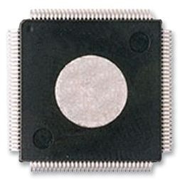
The MB9BF414R is a highly integrated 32-bit microcontrollers dedicated for embedded controllers with high-performance and competitive cost. These series are based on the ARM Cortex-M3 Processor with on-chip Flash memory and SRAM, and has peripheral functions such as Motor Control Timers, ADCs and Communication Interfaces (CAN, UART, CSIO, I2C, LIN).
- 32-bit ARM Cortex-M3 Core
- Processor version: r2p1
- Up to 144MHz Frequency Operation
- Memory Protection Unit (MPU): improves the reliability of an embedded system
- Integrated Nested Vectored Interrupt Controller (NVIC): 1 NMI (non-maskable interrupt) and 48 peripheral interrupts and 16 priority levels
- 24-bit System timer (Sys Tick): System timer for OS task management
- On-chip Memories [Flash memory] These series are based on two independent on-chip Flash memories.
- MainFlash
- Up to 512 Kbyte
- Built-in Flash Accelerator System with 16 Kbyte trace buffer memory
- The read access to Flash memory can be achieved without wait cycle up to operation frequency of 72MHz. Even at the operation frequency more than 72 MHz, an equivalent access to Flash memory can be obtained by Flash Accelerator System.
- Security function for code protection
- WorkFlash
- 32 Kbyte
- Read cycle
- 4 wait-cycle: the operation frequency more than 72 MHz
- 2 wait-cycle: the operation frequency more than 40 MHz, and to 72 MHz
- 0 wait-cycle: the operation frequency to 40 MHz
- Security function is shared with code protection [SRAM] This Series contain a total of up to 64Kbyte on-chip SRAM. This is composed of two independent SRAM (SRAM0, SRAM1). SRAM0 is connected to I-code bus and D-code bus of Cortex-M3 core. SRAM1 is connected to System bus.
- SRAM0: Up to 32 Kbyte
- SRAM1: Up to 32 Kbyte
- External Bus Interface
- Supports SRAM, NOR and NAND Flash device
- Up to 8 chip selects
- 8-/16-bit Data width
- Up to 25-bit Address bit
- Maximum area size : Up to 256 Mbytes
- Supports Address/Data multiplex
- Supports external RDY input CAN Interface (Max two channels)
- Compatible with CAN Specification 2.0A/B
- Maximum transfer rate: 1 Mbps
- Built-in 32 message buffer
- Multi-function Serial Interface (Max eight channels)
- 4 channels with 16 steps -9-bit FIFO (ch.4 to ch.7), 4 channels without FIFO (ch.0 to ch.3)
- DMA Controller (Eight channels) DMA Controller has an independent bus for CPU, so CPU and DMA Controller can process simultaneously.
- 8 independently configured and operated channels
- Transfer can be started by software or request from the built-in peripherals
- Transfer address area: 32-bit (4 Gbyte)
- Transfer mode: Block transfer/Burst transfer/Demand transfer
- Transfer data type: byte/half-word/word
- Transfer block count: 1 to 16
- Number of transfers: 1 to 65536
- A/D Converter (Max 16 channels) [12-bit A/D Converter]
- Successive Approximation Register type
- Built-in 3 unit
- Conversion time: 1.0 us @ 5 V
- Priority conversion available (priority at 2 levels)
- Scanning conversion mode
- Built-in FIFO for conversion data storage (for SCAN conversion: 16steps, for Priority conversion: 4steps)
- Base Timer (Max eight channels) Operation mode is selectable from the followings for each channel.
- 16-bit PWM timer
- 16-bit PPG timer
- 16-/32-bit reload timer
- 16-/32-bit PWC timer
- Multi-function Timer (Max three units)
- Dual Timer (32-/16-bit Down Counter) The Dual Timer consists of two programmable 32-/16-bit down counters. Operation mode is selectable from the followings for each channel