Описание
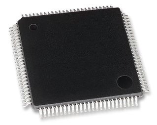
The TMS470R1A128(2)devices are members of the Texas Instruments (TI) TMS470R1x family of general-purpose16/32-bit reduced instruction set computer (RISC) microcontrollers. The TMS470R1x microcontroller offers high performance utilizingthe high-speed ARM7TDMI 16/32-bit RISC central processing unit (CPU), resulting in a high instruction throughput while maintaining greater code efficiency. The ARM7TDMI 16/32-bit RISC CPU views memory as a linear collection of bytes numbered upwards from zero. The A128 utilizes the big-endian format, where the most significant byte of a word is stored at the lowest numbered byte and the least significant byte at the highest numbered byte. High-end embedded control applications demand more performance from their controllers while maintaining low costs. The A128 RISC core architecture offers solutions to these performance and cost demands while maintaining low power consumption.The A128 devices contain the following:ARM7TDMI 16/32-Bit RISC CPUTMS470R1x system module (SYS) with 470+ enhancements128K-byte flash8K-byte SRAMZero-pin phase-locked loop (ZPLL) clock moduleAnalog watchdog (AWD) timerReal-time interrupt (RTI) moduleTwo serial peripheral interface (SPI) modulesTwo serial communications interface (SCI) modulesStandard CAN controller (SCC)Class II serial interface (C2SIa)10-bit, 16-input channel multi-buffered analog-to-digital converter (MibADC)High-end timer (HET) controlling 16 I/OsExternal Clock Prescale (ECP)Up to 49 I/O pins and 1 input-only pin The functions performed by the 470+ system module (SYS) include: Address decodingMemory protectionMemory and peripherals bus supervisionReset and abort exception managementPrioritization for all internal interrupt sourcesDevice clock controlParallel signature analysis (PSA)This data sheet includes device-specific information such as memory and peripheral select assignment, interrupt priority, and a device memory map. For a more detailed functional description of the SYS module, see the TMS470R1x System Module Reference Guide (literature number SPNU189).The A128 memory includes general-purpose SRAM supporting single-cycle read/write accesses in byte, halfword, and word modes.The flash memory on the A128 devices is a nonvolatile, electrically erasable and programmable memory implemented with a 32-bit-wide data bus interface.The flash operates with a system clock frequency of up to 28 MHz. In pipeline mode, the flash operates with a system clock frequency of up to 48 MHz. For more detailed information on the flash, see the F05 flash section of this data sheet and the TMS470R1x F05 Flash Reference Guide (literature number SPNU213).
- 28-MHz System Clock (48-MHz Pipeline Mode)
- Independent 16/32-Bit Instruction Set
- Open Architecture With Third-Party Support
- Built-In Debug Module
- Big-Endian Format Utilized
- 128K-Byte Program Flash
- One Bank With Ten Contiguous Sectors
- Internal State Machine for Programming and Erase
- 8K-Byte Static RAM (SRAM)
- Core Supply Voltage (VCC): 1.81 V-2.05 V
- I/O Supply Voltage (VCCIO): 3.0 V-3.6 V
- Low-Power Modes: STANDBY and HALT
- Extended Industrial Temperature Ranges
- 32-Bit Address Space Decoding
- Bus Supervision for Memory and Peripherals
- Analog Watchdog (AWD) Timer
- Real-Time Interrupt (RTI)
- System Integrity and Failure Detection
- Multiply-by-4 or -8 Internal ZPLL Option
- ZPLL Bypass Mode
- Two Serial Peripheral Interfaces (SPIs)
- 255 Programmable Baud Rates
- Two Serial Communications Interfaces (SCIs)
- 224 Selectable Baud Rates
- Asynchronous/Isosynchronous Modes
- Standard CAN Controller (SCC)
- 16-Mailbox Capacity
- Fully Compliant with CAN Protocol, Version 2.0B
- Class II Serial Interface (C2SIa)
- Two Selectable Data Rates
- Normal Mode 10.4 Kbps and 4X Mode 41.6 Kbps
- 16 Programmable I/O Channels:
- 14 High-Resolution Pins
- 2 Standard-Resolution Pins
- High-Resolution Share Feature (XOR)
- HET RAM (64-Instruction Capacity)
- 64-Word FIFO Buffer
- Single- or Continuous-Conversion Modes
- 1.55 µs Minimum Sample and Conversion Time
- Calibration Mode and Self-Test Features
- Programmable Low-Frequency External Clock (CLK)