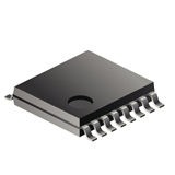
Analog Switch Triple SPDT 16-Pin TSSOP T/R, NX3L4053PW-Q100J, NXP

The NX3L4053-Q100 is a triple low-ohmic single-pole double-throw analog switch, suitable for use as an analog or digital multiplexer/demultiplexer. Each switch has a digital select input (nS), two independent inputs/outputs (nY0 and nY1) and a common input/output (nZ). All three switches share an enable input (E). A digital enable pin E is common to all switches. When E is HIGH, the switches are turned off. Schmitt trigger action at the digital inputs makes the circuit tolerant to slower input rise and fall times. Low threshold digital inputs allow this device to be driven by 1.8 V logic levels in 3.3 V applications without significant increase in supply current ICC. This makes it possible for the NX3L4053-Q100 to switch 4.3 V signals with a 1.8 V digital controller, eliminating the need for logic level translation. The NX3L4053-Q100 allows signals with amplitude up to VCC to be transmitted from nZ to nY0 or nY1; or from nY0 or nY1 to nZ. Its low ON resistance (0.5 O) and flatness (0.13 O) ensures minimal attenuation and distortion of transmitted signals. This product has been qualified to the Automotive Electronics Council (AEC) standard Q100 (Grade 1) and is suitable for use in automotive applications.

  • Automotive product qualification in accordance with AEC-Q100 (Grade 1)
    • Specified from -40 °C to +85 °C and from -40 °C to +125 °C
  • Wide supply voltage range from 1.4 V to 4.3 V
  • Very low ON resistance (peak):
    • 1.8 O (typical) at VCC = 1.4 V
    • 1.0 O( typical) at VCC = 1.65 V
    • 0.6 O (typical) at VCC = 2.3 V
    • 0.6 O (typical) at VCC = 2.7 V
    • 0.5 O (typical) at VCC = 4.3 V
  • Break-before-make switching
  • High noise immunity
  • ESD protection:
    • MIL-STD-883, method 3015 Class 3A exceeds 4000 V
    • HBM JESD22-A114F Class 3A exceeds 4000 V
    • MM JESD22-A115-A exceeds 200 V (C = 200 pF, R = 0 O)
    • CDM AEC-Q100-011 revision B exceeds 1000 V
    • IEC61000-4-2 contact discharge exceeds 6000 V for switch ports
  • CMOS low-power consumption
  • Latch-up performance exceeds 100 mA per JESD 78 Class II Level A
  • 1.8 V control logic at VCC = 3.6 V
  • Control input accepts voltages above supply voltage
  • Very low supply current, even when input is below VCC
  • High current handling capability (350 mA continuous current under 3.3 V supply)

Характеристики

Бренд

Number_of_inputs_per_chip

3

Number_of_outputs_per_chip

6

Operating_supply_current

0.00015@4.3V mA

Operating_supply_voltage

1.4, 3.3 V, 4.3

Operating_temp

-40 to 125 °C

Output_signal_type

Single-Ended

Pin_count

16

Polarity

Non-Inverting

Power_supply_type

Single

Product_dimensions

5.1(Max) x 4.5(Max) x 0.95(Max)

Schedule_b

8542390000

Screening_level

Automotive

Specifications

https://4donline.ihs.com/images/VipMasterIC/IC/PHGL/PHGLS28082/PHGLS28082-1.pdf?hkey=52A5661711E402568146F3353EA87419

Supplier_package

TSSOP

Number_of_channels_per_chip

3

Msl_level

1

Chip_enable_signals

Yes

Конфигурация

Triple SPDT

Country_of_origin

Thailand

Eccn

EAR99

Htsn

8542390001

Input_signal_type

Single

Kind

Analog Switch

Lead_finish

Gold Over Nickel Palladium

Mounting

Surface Mount

Max_frequency_25_deg_c_vcc

60@4.3 MHz

Max_on_resistance

1.8@1.4V Ohm

Max_power_dissipation

500 mW

Max_processing_temp

260

Max_turn_on_time

90@1.6V ns

SKU: NX3L4053PW-Q100J

Description

The NX3L4053-Q100 is a triple low-ohmic single-pole double-throw analog switch, suitable for use as an analog or digital multiplexer/demultiplexer. Each switch has a digital select input (nS), two independent inputs/outputs (nY0 and nY1) and a common input/output (nZ). All three switches share an enable input (E). A digital enable pin E is common to all switches. When E is HIGH, the switches are turned off. Schmitt trigger action at the digital inputs makes the circuit tolerant to slower input rise and fall times. Low threshold digital inputs allow this device to be driven by 1.8 V logic levels in 3.3 V applications without significant increase in supply current ICC. This makes it possible for the NX3L4053-Q100 to switch 4.3 V signals with a 1.8 V digital controller, eliminating the need for logic level translation. The NX3L4053-Q100 allows signals with amplitude up to VCC to be transmitted from nZ to nY0 or nY1; or from nY0 or nY1 to nZ. Its low ON resistance (0.5 O) and flatness (0.13 O) ensures minimal attenuation and distortion of transmitted signals. This product has been qualified to the Automotive Electronics Council (AEC) standard Q100 (Grade 1) and is suitable for use in automotive applications.

  • Automotive product qualification in accordance with AEC-Q100 (Grade 1)
    • Specified from -40 °C to +85 °C and from -40 °C to +125 °C
  • Wide supply voltage range from 1.4 V to 4.3 V
  • Very low ON resistance (peak):
    • 1.8 O (typical) at VCC = 1.4 V
    • 1.0 O( typical) at VCC = 1.65 V
    • 0.6 O (typical) at VCC = 2.3 V
    • 0.6 O (typical) at VCC = 2.7 V
    • 0.5 O (typical) at VCC = 4.3 V
  • Break-before-make switching
  • High noise immunity
  • ESD protection:
    • MIL-STD-883, method 3015 Class 3A exceeds 4000 V
    • HBM JESD22-A114F Class 3A exceeds 4000 V
    • MM JESD22-A115-A exceeds 200 V (C = 200 pF, R = 0 O)
    • CDM AEC-Q100-011 revision B exceeds 1000 V
    • IEC61000-4-2 contact discharge exceeds 6000 V for switch ports
  • CMOS low-power consumption
  • Latch-up performance exceeds 100 mA per JESD 78 Class II Level A
  • 1.8 V control logic at VCC = 3.6 V
  • Control input accepts voltages above supply voltage
  • Very low supply current, even when input is below VCC
  • High current handling capability (350 mA continuous current under 3.3 V supply)

Additional information

Бренд

Number_of_inputs_per_chip

3

Number_of_outputs_per_chip

6

Operating_supply_current

0.00015@4.3V mA

Operating_supply_voltage

1.4, 3.3 V, 4.3

Operating_temp

-40 to 125 °C

Output_signal_type

Single-Ended

Pin_count

16

Polarity

Non-Inverting

Power_supply_type

Single

Product_dimensions

5.1(Max) x 4.5(Max) x 0.95(Max)

Schedule_b

8542390000

Screening_level

Automotive

Specifications

https://4donline.ihs.com/images/VipMasterIC/IC/PHGL/PHGLS28082/PHGLS28082-1.pdf?hkey=52A5661711E402568146F3353EA87419

Supplier_package

TSSOP

Number_of_channels_per_chip

3

Msl_level

1

Chip_enable_signals

Yes

Конфигурация

Triple SPDT

Country_of_origin

Thailand

Eccn

EAR99

Htsn

8542390001

Input_signal_type

Single

Kind

Analog Switch

Lead_finish

Gold Over Nickel Palladium

Mounting

Surface Mount

Max_frequency_25_deg_c_vcc

60@4.3 MHz

Max_on_resistance

1.8@1.4V Ohm

Max_power_dissipation

500 mW

Max_processing_temp

260

Max_turn_on_time

90@1.6V ns