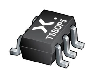
Analog Switch Single SPST 5-Pin TSSOP T/R, 74AHCT1G66GW,125, Nexperia
74AHC1G66 and 74AHCT1G66 are high-speed Si-gate CMOS devices. They are single-pole single-throw analog switches. The switch has two input/output pins (Y and Z) and an active HIGH enable input pin (E). When pin E is LOW, the analog switch is turned off.
- Very low ON resistance:
- 26 O (typ.) at VCC = 3.0 V
- 16 O (typ.) at VCC = 4.5 V
- 14 O (typ.) at VCC = 5.5 V
- High noise immunity
- Low power dissipation
- Balanced propagation delays
- Multiple package options
- ESD protection:
- HMB JESD22-A114E exceeds 2000 V
- MM JESD22-A115-A exceeds 200 V
- CDM JESD22-C101C exceeds 1000 V
- Specified from -40 Cel to +85 Cel and -40 Cel to +125 Cel
Характеристики
| Бренд |
Nexperia
|
| Country_of_origin |
Malaysia
|
| Eccn |
EAR99
|
| Htsn |
8542390001
|
| Input_signal_type |
Single
|
| Kind |
Analog Switch
|
| Lead_finish |
Tin
|
| Max_high_lev_output_current |
25 mA
|
| Max_on_resistance |
110@3.6V Ohm
|
| Max_low_lev_output_current |
25 mA
|
| Max_power_dissipation |
250 mW
|
| Max_processing_temp |
260
|
| Max_propagation_delay_btb |
1@5.5V ns
|
| Max_turn_on_time |
10@5.5V ns
|
| Mounting |
Surface Mount
|
| Msl_level |
1
|
| Конфигурация |
Single SPST
|
| Operating_temp |
-40 to 125 °C
|
| Schedule_b |
8542390000
|
| Number_of_inputs_per_chip |
1
|
| Operating_supply_voltage |
4.5, 5 V, 5.5
|
| Operating_supply_current |
75 mA
|
| Max_on_resistance_range |
100 to 150 Ohm
|
| Supplier_package |
TSSOP
|
| Number_of_outputs_per_chip |
1
|
| Specifications |
https://4donline.ihs.com/images/VipMasterIC/IC/PHGL/PHGLS18301/PHGLS18301-1.pdf?hkey=52A5661711E402568146F3353EA87419
|
| Chip_enable_signals |
Yes
|
| Propagat_delay_test_condit |
50 pF
|
| Product_dimensions |
2.25 x 1.35 x 1 mm
|
| Power_supply_type |
Single
|
| Polarity |
Non-Inverting
|
| Pin_count |
5
|
| Output_signal_type |
Single-Ended
|
| Number_of_channels_per_chip |
1
|
Артикул: 74AHCT1G66GW,125
