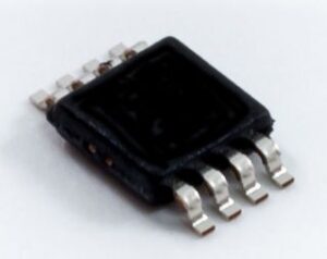
Analog Switch Dual SPST 8-Pin VSSOP T/R, 74LVC2G66DC,125, Nexperia

The 74LVC2G66 is a low-power, low-voltage, high-speed Si-gate CMOS device. The 74LVC2G66 provides two single pole, single-throw analog switch functions. Each switch has two input/output terminals (nY and nZ) and an active HIGH enable input (nE). When nE is LOW, the analog switch is turned off. Schmitt-trigger action at the enable inputs makes the circuit tolerant of slower input rise and fall times across the entire VCC range from 1.65 V to 5.5 V.

  • Wide supply voltage range from 1.65 V to 5.5 V
  • Very low ON resistance:
    • 7.5 ? (typical) at VCC = 2.7 V
    • 6.5 ? (typical) at VCC = 3.3 V
    • 6 ? (typical) at VCC = 5 V
  • Switch current capability of 32 mA
  • High noise immunity
  • CMOS low power consumption
  • TTL interface compatibility at 3.3 V
  • Latch-up performance meets requirements of JESD78 Class I
  • ESD protection:
    • HBM JESD22-A114F exceeds 2000 V
    • MM JESD22-A115-A exceeds 200 V
  • Enable input accepts voltages up to 5.5 V
  • Multiple package options
  • Specified from –40 ? to +85 ? and –40 ? to +125 ?
Характеристики

Бренд

Operating_temp

-40 to 125 °C

Output_signal_type

Single-Ended

Pin_count

8

Polarity

Non-Inverting

Power_supply_type

Single

Product_dimensions

2.1 x 2.4 x 0.85 mm

Propagat_delay_test_condit

50 pF

Schedule_b

8542390000

Specifications

https://4donline.ihs.com/images/VipMasterIC/IC/PHGL/PHGLS27077/PHGLS27077-1.pdf?hkey=52A5661711E402568146F3353EA87419

Number_of_outputs_per_chip

2

Supplier_package

VSSOP

Max_on_resistance_range

150 to 250 Ohm

Operating_supply_current

0.2@5.5V

Operating_supply_voltage

1.65 V, 5.5

Number_of_inputs_per_chip

2

Chip_enable_signals

Yes

Конфигурация

Dual SPST

Country_of_origin

Taiwan

Eccn

EAR99

Htsn

8542390001

Input_signal_type

Single

Kind

Analog Switch

Lead_finish

Gold

Max_high_lev_output_current

50 mA

Max_low_lev_output_current

50 mA

Max_on_resistance

195@1.95V Ohm

Max_power_dissipation

250 mW

Max_processing_temp

260

Max_propagation_delay_btb

0.2@5.5 ns, 0.3@3.6, 0.4@2.7, 0.8@1.95

Max_turn_on_time

4.6@1.95V ns

Mounting

Surface Mount

Msl_level

1

Number_of_channels_per_chip

2

Артикул: 74LVC2G66DC,125

Описание

The 74LVC2G66 is a low-power, low-voltage, high-speed Si-gate CMOS device. The 74LVC2G66 provides two single pole, single-throw analog switch functions. Each switch has two input/output terminals (nY and nZ) and an active HIGH enable input (nE). When nE is LOW, the analog switch is turned off. Schmitt-trigger action at the enable inputs makes the circuit tolerant of slower input rise and fall times across the entire VCC range from 1.65 V to 5.5 V.

  • Wide supply voltage range from 1.65 V to 5.5 V
  • Very low ON resistance:
    • 7.5 ? (typical) at VCC = 2.7 V
    • 6.5 ? (typical) at VCC = 3.3 V
    • 6 ? (typical) at VCC = 5 V
  • Switch current capability of 32 mA
  • High noise immunity
  • CMOS low power consumption
  • TTL interface compatibility at 3.3 V
  • Latch-up performance meets requirements of JESD78 Class I
  • ESD protection:
    • HBM JESD22-A114F exceeds 2000 V
    • MM JESD22-A115-A exceeds 200 V
  • Enable input accepts voltages up to 5.5 V
  • Multiple package options
  • Specified from –40 ? to +85 ? and –40 ? to +125 ?
Детали

Бренд

Operating_temp

-40 to 125 °C

Output_signal_type

Single-Ended

Pin_count

8

Polarity

Non-Inverting

Power_supply_type

Single

Product_dimensions

2.1 x 2.4 x 0.85 mm

Propagat_delay_test_condit

50 pF

Schedule_b

8542390000

Specifications

https://4donline.ihs.com/images/VipMasterIC/IC/PHGL/PHGLS27077/PHGLS27077-1.pdf?hkey=52A5661711E402568146F3353EA87419

Number_of_outputs_per_chip

2

Supplier_package

VSSOP

Max_on_resistance_range

150 to 250 Ohm

Operating_supply_current

0.2@5.5V

Operating_supply_voltage

1.65 V, 5.5

Number_of_inputs_per_chip

2

Chip_enable_signals

Yes

Конфигурация

Dual SPST

Country_of_origin

Taiwan

Eccn

EAR99

Htsn

8542390001

Input_signal_type

Single

Kind

Analog Switch

Lead_finish

Gold

Max_high_lev_output_current

50 mA

Max_low_lev_output_current

50 mA

Max_on_resistance

195@1.95V Ohm

Max_power_dissipation

250 mW

Max_processing_temp

260

Max_propagation_delay_btb

0.2@5.5 ns, 0.3@3.6, 0.4@2.7, 0.8@1.95

Max_turn_on_time

4.6@1.95V ns

Mounting

Surface Mount

Msl_level

1

Number_of_channels_per_chip

2