Описание
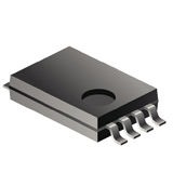
The 74LVC1G53-Q100 is a low-power, low-voltage, high-speed, Si-gate CMOS device. The 74LVC1G53-Q100 provides one analog multiplexer/demultiplexer with a digital select input (S), two independent inputs/outputs (Y0 and Y1), a common input/output (Z) and an active LOW enable input (E). When pin E is HIGH, the switch is turned off. Schmitt-trigger action at the select and enable inputs makes the circuit tolerant to slower input rise and fall times across the entire VCC range from 1.65 V to 5.5 V. This product has been qualified to the Automotive Electronics Council (AEC) standard Q100 (Grade 1) and is suitable for use in automotive applications.
- Automotive product qualification in accordance with AEC-Q100 (Grade 1)
- Specified from -40 °C to +85 °C and from -40 °C to +125 °C
- Wide supply voltage range from 1.65 V to 5.5 V
- Very low ON resistance:
- 7.5 O (typical) at VCC = 2.7 V
- 6.5 O (typical) at VCC = 3.3 V
- 6 O (typical) at VCC = 5 V
- Switch current capability of 32 mA
- High noise immunity
- CMOS low power consumption
- TTL interface compatibility at 3.3 V
- Latch-up performance meets requirements of JESD 78 Class I
- Multiple package options
- ESD protection:
- MIL-STD-883, method 3015 exceeds 2000 V
- HBM JESD22-A114F exceeds 2000 V
- MM JESD22-A115-A exceeds 200 V (C = 200 pF, R = 0 O)
