Описание
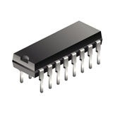
The HEF4052B is a dual 4-channel analog multiplexer/demultiplexer with common channel select logic. Each multiplexer/demultiplexer has four independent inputs/outputs (nY0 to nY3) and a common input/output (nZ). The common channel select logic includes two select inputs (S1 and S2) and an active LOW enable input (E). Both multiplexers/demultiplexers contain four bidirectional analog switches, each with one side connected to an independent input/output (nY0 to nY3) and the other side connected to a common input/output (nZ). With E LOW, one of the four switches is selected (low-impedance ON-state) by S1 and S2. With E HIGH, all switches are in the high-impedance OFF-state, independent of S1 and S2. If break before make is needed, then it is necessary to use the enable input. VDD and VSS are the supply voltage connections for the digital control inputs (S1 and S2, and E). The VDD to VSS range is 3 V to 15 V. The analog inputs/outputs (nY0 to nY3, and nZ) can swing between VDD as a positive limit and VEE as a negative limit. VDD- VEE may not exceed 15 V. Unused inputs must be connected to VDD, VSS, or another input. For operation as a digital multiplexer/demultiplexer, VEE is connected to VSS (typically ground). VEE and VSS are the supply voltage connections for the switches.
- Fully static operation
- 5 V, 10 V, and 15 V parametric ratings
- Standardized symmetrical output characteristics
- Specified from -40 ? to +85 ? and -40 ? to +125 ?
- Complies with JEDEC standard JESD 13-B