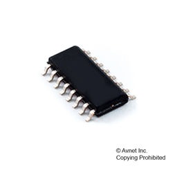
Analog Multiplexer Triple 2:1 16-Pin SO Tube, 74LV4053D,112, Nexperia

The 74LV4053 is a triple single-pole double-throw (SPDT) analog switch, suitable for use as an analog or digital multiplexer/demultiplexer. It is a low-voltage Si-gate CMOS device and is pin and function compatible with the 74HC4053 and 74HCT4053. Each switch has a digital select input (Sn), two independent inputs/outputs (nY0 and nY1) and a common input/output (nZ). All three switches share an enable input (E). A HIGH on E causes all switches into the high-impedance OFF-state, independent of Sn. VCC and GND are the supply voltage connections for the digital control inputs (Sn and E). The VCC to GND range is 1 V to 6 V. The analog inputs/outputs (nY0, nY1 and nZ) can swing between VCC as a positive limit and VEE as a negative limit. VCC- VEE may not exceed 6 V. For operation as a digital multiplexer/demultiplexer, VEE is connected to GND (typically ground). VEE and VSS are the supply voltage connections for the switches.

  • Optimized for low-voltage applications: 1.0 V to 3.6 V
  • Accepts TTL input levels between VCC = 2.7 V and VCC = 3.6 V
  • Low ON resistance:
    • 180 ? (typical) at VCC – VEE = 2.0 V
    • 100 ? (typical) at VCC – VEE = 3.0 V
    • 75 ? (typical) at VCC – VEE = 4.5 V
  • Logic level translation:
    • To enable 3 V logic to communicate with ±3 V analog signals
  • Typical ‘break before make’ built in
  • ESD protection:
    • HBM JESD22-A114-C exceeds 2000 V
    • MM JESD22-A115-A exceeds 200 V
  • Multiple package options
  • Specified from -40 ? to +85 ? and from -40 ? to +125 ?
Характеристики

Бренд

Chip_enable_signals

Yes

Max_on_resistance

435@2V Ohm

Number_of_channels_per_chip

3

Number_of_outputs_per_chip

3

Max_turn_on_time

125@1.2V ns

Output_signal_type

Single-Ended

Power_supply_type

Single

Max_propagation_delay_btb

25@1.2, 3@6 ns, 4@4.5, 5@3.3, 6@2.7, 9@2

Propagat_delay_test_condit

50 pF

Max_low_lev_output_current

25 mA

Max_on_resist_range

400 to 1000 Ohm

Number_of_inputs_per_chip

6

Max_high_lev_output_current

25 mA

Msl_level

1

Конфигурация

Triple 2:1

Country_of_origin

China

Eccn

EAR99

Htsn

8542390001

Input_signal_type

Single

Kind

Analog Multiplexer

Lead_finish

Gold

Max_power_dissipation

500 mW

Max_processing_temp

260

Mounting

Surface Mount

Operat_supply_current

0.08@6V@-40C to 125C mA

Operat_supply_voltage

1, 3.3 V, 6

Operat_temperature

-40 to 125 °C

Pin_count

16

Product_dimensions

10 x 4 x 1.45 mm

Schedule_b

8542390000

Specifications

https://4donline.ihs.com/images/VipMasterIC/IC/NEXP/NEXP-S-A0003511301/NEXP-S-A0003511301-1.pdf?hkey=52A5661711E402568146F3353EA87419

Supplier_package

SO

Артикул: 74LV4053D,112

Описание

The 74LV4053 is a triple single-pole double-throw (SPDT) analog switch, suitable for use as an analog or digital multiplexer/demultiplexer. It is a low-voltage Si-gate CMOS device and is pin and function compatible with the 74HC4053 and 74HCT4053. Each switch has a digital select input (Sn), two independent inputs/outputs (nY0 and nY1) and a common input/output (nZ). All three switches share an enable input (E). A HIGH on E causes all switches into the high-impedance OFF-state, independent of Sn. VCC and GND are the supply voltage connections for the digital control inputs (Sn and E). The VCC to GND range is 1 V to 6 V. The analog inputs/outputs (nY0, nY1 and nZ) can swing between VCC as a positive limit and VEE as a negative limit. VCC- VEE may not exceed 6 V. For operation as a digital multiplexer/demultiplexer, VEE is connected to GND (typically ground). VEE and VSS are the supply voltage connections for the switches.

  • Optimized for low-voltage applications: 1.0 V to 3.6 V
  • Accepts TTL input levels between VCC = 2.7 V and VCC = 3.6 V
  • Low ON resistance:
    • 180 ? (typical) at VCC – VEE = 2.0 V
    • 100 ? (typical) at VCC – VEE = 3.0 V
    • 75 ? (typical) at VCC – VEE = 4.5 V
  • Logic level translation:
    • To enable 3 V logic to communicate with ±3 V analog signals
  • Typical ‘break before make’ built in
  • ESD protection:
    • HBM JESD22-A114-C exceeds 2000 V
    • MM JESD22-A115-A exceeds 200 V
  • Multiple package options
  • Specified from -40 ? to +85 ? and from -40 ? to +125 ?
Детали

Бренд

Chip_enable_signals

Yes

Max_on_resistance

435@2V Ohm

Number_of_channels_per_chip

3

Number_of_outputs_per_chip

3

Max_turn_on_time

125@1.2V ns

Output_signal_type

Single-Ended

Power_supply_type

Single

Max_propagation_delay_btb

25@1.2, 3@6 ns, 4@4.5, 5@3.3, 6@2.7, 9@2

Propagat_delay_test_condit

50 pF

Max_low_lev_output_current

25 mA

Max_on_resist_range

400 to 1000 Ohm

Number_of_inputs_per_chip

6

Max_high_lev_output_current

25 mA

Msl_level

1

Конфигурация

Triple 2:1

Country_of_origin

China

Eccn

EAR99

Htsn

8542390001

Input_signal_type

Single

Kind

Analog Multiplexer

Lead_finish

Gold

Max_power_dissipation

500 mW

Max_processing_temp

260

Mounting

Surface Mount

Operat_supply_current

0.08@6V@-40C to 125C mA

Operat_supply_voltage

1, 3.3 V, 6

Operat_temperature

-40 to 125 °C

Pin_count

16

Product_dimensions

10 x 4 x 1.45 mm

Schedule_b

8542390000

Specifications

https://4donline.ihs.com/images/VipMasterIC/IC/NEXP/NEXP-S-A0003511301/NEXP-S-A0003511301-1.pdf?hkey=52A5661711E402568146F3353EA87419

Supplier_package

SO