Описание
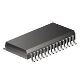
NOTE: The ADC10061 and ADC10062 are obsolete. They are described here for reference only.Using an innovative, patented multistep* conversion technique, these CMOS analog-to-digital converters offer sub-microsecond conversion times yet dissipate a maximum of only 235 mW. These converters perform 10-bit conversions in two lower-resolution “flashes”, yielding a fast A/D without the cost, power consumption, and other problems associated with true flash approaches.The analog input voltage is sampled and held by an internal sampling circuit. Input signals at frequencies from DC to over 200 kHz can, therefore, be digitized accurately without the need for an external sample-and-hold circuit.The ADC10062 and ADC10064 include a “speed-up” pin. Connecting an external resistor between this pin and ground reduces the typical conversion time to as little as 350 ns with only a small increase in linearity error.For ease of interface to microprocessors, the ADC10061, ADC10062, and ADC10064 have been designed to appear as a memory location or I/O port without the need for external interface logic.*U.S. Patent Number 4918449
