Описание
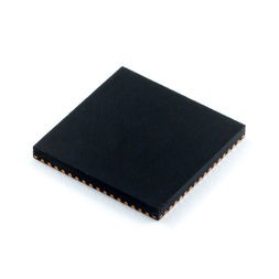
The ADS4249 is a member of the ADS42xx ultralow-power family of dual-channel, 12-bit and 14-bit analog-to-digital converters (ADCs). Innovative design techniques are used to achieve high dynamic performance, while consuming extremely low power with a 1.8-V supply. This topology makes the ADS4249 well-suited for multi-carrier, wide-bandwidth communications applications.The ADS4249 has gain options that can be used to improve SFDR performance at lower full-scale input ranges. This device also includes a dc offset correction loop that can be used to cancel the ADC offset. Both DDR LVDS and parallel CMOS digital output interfaces are available in a compact QFN-64 PowerPAD package.The device includes internal references while the traditional reference pins and associated decoupling capacitors have been eliminated. The ADS4249 is specified over the industrial temperature range (–40°C to 85°C).
- 560-mW Total Power at 250 MSPS
- 80-dBc SFDR at 170 MHz
- 71.7-dBFS SNR at 170 MHz
SNR/SFDR Trade-off
- 1.8-V Parallel CMOS Interface
- Double Data Rate (DDR) LVDS with
Programmable Swing:- Standard Swing: 350 mV
- Low Swing: 200 mV
Down to 200 mVPP
Lead (QFN) Package