Описание
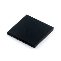
ADS62C15 is a dual channel 11-bit A/D converter with maximum sample rates up to 125 MSPS. It combines high performance and low power consumption in a compact 64 QFN package. Using an internal sample and hold and low jitter clock buffer, the ADC supports high SNR and high SFDR at high input frequencies. It has coarse and fine gain options that can be used to improve SFDR performance at lower full-scale input ranges.ADS62C15 uses proprietarytechnology that can be used to overcome SNR limitation due to quantization noise (for bandwidths less than Nyquist, Fs/2). It includes a digital processing block that consists of several useful and commonly used digital functions such as ADC offset correction, fine gain correction (in steps of 0.05 dB), decimation by 2,4,8 and in-built and custom programmable filters. By default, the digital processing block is bypassed, and its functions are disabled.Two output interface options exist – parallel CMOS and DDR LVDS (Double Data Rate). ADS62C15 includes internal references while traditional reference pins and associated decoupling capacitors have been eliminated. The device can also be driven with an external reference. The device is specified over the industrial temperature range (–40°C to 85°C).
using technology
up to 6 dB for SNR/SFDR Trade-Off
- Offset Correction
- Fine Gain Correction, in Steps of 0.05 dB
- Decimation by 2/4/8
- Built-in and Custom Programmable 24-Tap Low/High/
Band Pass Filters
Amplitude Down to 400 mVPP