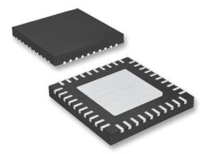
ADC Single Pipelined 80Msps 12-bit Parallel 40-Pin TQFN EP T/R, MAX1209ETL+T, Maxim Integrated

The MAX1209 is a 3.3V, 12-bit, 80Msps analog-to-digital converter (ADC) featuring a fully differential wideband track-and-hold (T/H) input amplifier, driving a low-noise internal quantizer. The analog input stage accepts single-ended or differential signals. The MAX1209 is optimized for low power, small size, and high dynamic performance. Excellent dynamic performance is maintained from baseband to input frequencies of 175MHz and beyond, making the MAX1209 ideal for intermediate-frequency (IF) sampling applications. Powered from a single 3.0V to 3.6V supply, the MAX1209 consumes only 393mW while delivering a typical signal-to-noise (SNR) performance of 66.5dB at an input frequency of 175MHz. In addition to low operating power, the MAX1209 features a 3µW power-down mode to conserve power during idle periods. A flexible reference structure allows the MAX1209 to use the internal 2.048V bandgap reference or accept an externally applied reference. The reference structure allows the full-scale analog input range to be adjusted from ±0.35V to ±1.15V. The MAX1209 provides a common-mode reference to simplify design and reduce external component count in differential analog input circuits. The MAX1209 supports both a single-ended and differential input clock drive. Wide variations in the clock duty cycle are compensated with the ADC"s internal duty-cycle equalizer (DCE). ADC conversion results are available through a 12-bit, parallel, CMOS-compatible output bus. The digital output format is pin selectable to be either two"s complement or Gray code. A data-valid indicator eliminates external components that are normally required for reliable digital interfacing. A separate digital power input accepts a wide 1.7V to 3.6V supply, allowing the MAX1209 to interface with various logic levels. The MAX1209 is available in a 6mm x 6mm x 0.8mm, 40-pin thin QFN package with exposed paddle (EP), and is specified for the extended industrial (-40°C to +85°C) temperature range. See a parametric table of the complete family of pin-compatible, 12-/14-bit high-speed ADCs.

  • Direct IF Sampling Up to 400MHz
  • Excellent Dynamic Performance
    • 68.0dB/66.5dB SNR at fIN = 70MHz/175MHz
    • 85.1dBc/85.5dBc SFDR at fIN = 70MHz/175MHz
  • 3.3V Low-Power Operation
    • 366mW (Single-Ended Clock Mode)
    • 393mW (Differential Clock Mode)
    • 3µW (Power-Down Mode)
  • Differential or Single-Ended Clock
  • Fully Differential or Single-Ended Analog Input
  • Adjustable Full-Scale Analog Input Range: ±0.35V to ±1.15V
  • Common-Mode Reference
  • CMOS-Compatible Outputs in Two"s Complement or Gray Code
  • Data-Valid Indicator Simplifies Digital Design
  • Data Out-of-Range Indicator
  • Miniature, 40-Pin Thin QFN Package with Exposed Paddle
  • Evaluation Kit Available (Order MAX1211EVKIT)
  • Характеристики

    Volt_supply_source

    Single

    Number_of_analog_inputs

    1

    Sampling_rate

    80 Msps

    Volt_reference

    External, Internal

    Typical_power_dissipation

    393 mW

    Differential_nonlinearity

    0.35 LSB

    Signal_to_noise_ratio

    68 dB

    Input_type

    Voltage

    Input_signal_type

    Differential

    Input_volt

    ±1.024 V

    Бренд

    Msl_level

    1

    Eccn

    EAR99

    Htsn

    8542390001

    Lead_finish

    Matte Tin

    Max_power_dissipation

    436 mW

    Max_processing_temp

    260, 300

    Mounting

    Surface Mount

    Operating_temp

    -40 to 85 °C

    Pin_count

    40

    Product_dimensions

    6 x 6 x 0.73 mm

    Schedule_b

    8542390000

    Screening_level

    Extended Industrial

    Specifications

    https://4donline.ihs.com/images/VipMasterIC/IC/MAXM/MAXMS07709/MAXMS07709-1.pdf?hkey=52A5661711E402568146F3353EA87419

    Supplier_package

    TQFN EP

    Number_of_adc_channels

    1

    Polarity_of_input_volt

    Bipolar

    Operating_supply_volt

    3, 3.3 V, 3.6

    Number_of_adcs

    1

    Digital_interface_type

    Parallel

    Артикул: MAX1209ETL+T

    Описание

    The MAX1209 is a 3.3V, 12-bit, 80Msps analog-to-digital converter (ADC) featuring a fully differential wideband track-and-hold (T/H) input amplifier, driving a low-noise internal quantizer. The analog input stage accepts single-ended or differential signals. The MAX1209 is optimized for low power, small size, and high dynamic performance. Excellent dynamic performance is maintained from baseband to input frequencies of 175MHz and beyond, making the MAX1209 ideal for intermediate-frequency (IF) sampling applications. Powered from a single 3.0V to 3.6V supply, the MAX1209 consumes only 393mW while delivering a typical signal-to-noise (SNR) performance of 66.5dB at an input frequency of 175MHz. In addition to low operating power, the MAX1209 features a 3µW power-down mode to conserve power during idle periods. A flexible reference structure allows the MAX1209 to use the internal 2.048V bandgap reference or accept an externally applied reference. The reference structure allows the full-scale analog input range to be adjusted from ±0.35V to ±1.15V. The MAX1209 provides a common-mode reference to simplify design and reduce external component count in differential analog input circuits. The MAX1209 supports both a single-ended and differential input clock drive. Wide variations in the clock duty cycle are compensated with the ADC"s internal duty-cycle equalizer (DCE). ADC conversion results are available through a 12-bit, parallel, CMOS-compatible output bus. The digital output format is pin selectable to be either two"s complement or Gray code. A data-valid indicator eliminates external components that are normally required for reliable digital interfacing. A separate digital power input accepts a wide 1.7V to 3.6V supply, allowing the MAX1209 to interface with various logic levels. The MAX1209 is available in a 6mm x 6mm x 0.8mm, 40-pin thin QFN package with exposed paddle (EP), and is specified for the extended industrial (-40°C to +85°C) temperature range. See a parametric table of the complete family of pin-compatible, 12-/14-bit high-speed ADCs.

    • Direct IF Sampling Up to 400MHz
    • Excellent Dynamic Performance
      • 68.0dB/66.5dB SNR at fIN = 70MHz/175MHz
      • 85.1dBc/85.5dBc SFDR at fIN = 70MHz/175MHz
  • 3.3V Low-Power Operation
    • 366mW (Single-Ended Clock Mode)
    • 393mW (Differential Clock Mode)
    • 3µW (Power-Down Mode)
  • Differential or Single-Ended Clock
  • Fully Differential or Single-Ended Analog Input
  • Adjustable Full-Scale Analog Input Range: ±0.35V to ±1.15V
  • Common-Mode Reference
  • CMOS-Compatible Outputs in Two"s Complement or Gray Code
  • Data-Valid Indicator Simplifies Digital Design
  • Data Out-of-Range Indicator
  • Miniature, 40-Pin Thin QFN Package with Exposed Paddle
  • Evaluation Kit Available (Order MAX1211EVKIT)
  • Детали

    Volt_supply_source

    Single

    Number_of_analog_inputs

    1

    Sampling_rate

    80 Msps

    Volt_reference

    External, Internal

    Typical_power_dissipation

    393 mW

    Differential_nonlinearity

    0.35 LSB

    Signal_to_noise_ratio

    68 dB

    Input_type

    Voltage

    Input_signal_type

    Differential

    Input_volt

    ±1.024 V

    Бренд

    Msl_level

    1

    Eccn

    EAR99

    Htsn

    8542390001

    Lead_finish

    Matte Tin

    Max_power_dissipation

    436 mW

    Max_processing_temp

    260, 300

    Mounting

    Surface Mount

    Operating_temp

    -40 to 85 °C

    Pin_count

    40

    Product_dimensions

    6 x 6 x 0.73 mm

    Schedule_b

    8542390000

    Screening_level

    Extended Industrial

    Specifications

    https://4donline.ihs.com/images/VipMasterIC/IC/MAXM/MAXMS07709/MAXMS07709-1.pdf?hkey=52A5661711E402568146F3353EA87419

    Supplier_package

    TQFN EP

    Number_of_adc_channels

    1

    Polarity_of_input_volt

    Bipolar

    Operating_supply_volt

    3, 3.3 V, 3.6

    Number_of_adcs

    1

    Digital_interface_type

    Parallel