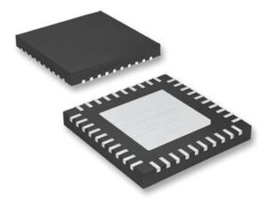
ADC Single Pipelined 65Msps 12-bit Parallel 40-Pin TQFN EP, MAX1211ETL+, Maxim Integrated

The MAX1211 is a 3.3V, 12-bit analog-to-digital converter (ADC) featuring a fully differential wideband track-and-hold (T/H) input, driving the internal quantizer. The MAX1211 is optimized for low power, small size, and high dynamic performance in intermediate frequency (IF) sampling applications. This ADC operates from a single 3.0V to 3.6V supply, consuming only 340mW while delivering a typical signal-to-noise ratio (SNR) performance of 66.8dB at a 175MHz input frequency. The T/H-driven input stage accepts single-ended or differential inputs. In addition to low operating power, the MAX1211 features a 0.15mW power-down mode to conserve power during idle periods. A flexible reference structure allows the MAX1211 to use its internal precision bandgap reference or accept an externally applied reference. A common-mode reference is provided to simplify design and reduce external component count in differential analog input circuits. The MAX1211 supports both a single-ended and differential input clock drive. Wide variations in the clock duty cycle are compensated with the ADC"s internal duty-cycle equalizer. The MAX1211 features parallel, CMOS-compatible outputs. The digital output format is pin selectable to be either two"s complement or Gray code. A data-valid indicator eliminates external components that are normally required for reliable digital interfacing. A separate power input for the digital outputs accepts a voltage from 1.7V to 3.6V for flexible interfacing with various logic levels. The MAX1211 is available in a 6mm x 6mm x 0.8mm, 40- pin thin QFN package with exposed paddle (EP), and is specified for the extended industrial (-40°C to +85°C) temperature range. See a parametric table of the complete family of pin-compatible, 12-/14-bit high-speed ADCs.

  • Direct IF Sampling Up to 400MHz
  • 700MHz Input Bandwidth
  • Excellent Dynamic Performance
    • 66.8dB SNR at fIN = 175MHz
    • 79.7dBc SFDR at fIN = 175MHz
  • 3.3V Low-Power Operation
    • 314mW (Single-Ended Clock Mode)
    • 340mW (Differential Clock Mode)
  • Differential or Single-Ended Clock
  • Accepts 20% to 80% Clock Duty Cycle
  • Fully Differential or Single-Ended Analog Input
  • Adjustable Full-Scale Analog Input Range
  • Common-Mode Reference
  • Power-Down Mode
  • CMOS-Compatible Outputs in Two"s Complementor Gray Code
  • Data-Valid Indicator Simplifies Digital Interface
  • Out-of-Range Indicator
  • Miniature, 40-Pin Thin QFN Package with ExposedPaddle
  • Evaluation Kit Available (Order MAX1211EVKIT)
  • Характеристики

    Volt_supply_source

    Single

    Number_of_analog_inputs

    1

    Sampling_rate

    65 Msps

    Volt_reference

    External, Internal

    Digital_supply_support

    No

    Architecture

    Pipelined

    Resolution

    12 Bit

    Typical_power_dissipation

    340 mW

    Differential_nonlinearity

    0.75 LSB

    Signal_to_noise_ratio

    68.5 dB

    Input_type

    Voltage

    Input_signal_type

    Differential, Single-Ended

    Input_volt

    ±1.024 V

    Бренд

    Msl_level

    1

    Eccn

    3A991.C.2

    Htsn

    8542390001

    Lead_finish

    Matte Tin

    Max_power_dissipation

    379 mW

    Max_processing_temp

    260, 300

    Mounting

    Surface Mount

    Operating_temp

    -40 to 85 °C

    Pin_count

    40

    Product_dimensions

    6 x 6 x 0.73 mm

    Schedule_b

    8542390000

    Screening_level

    Extended Industrial

    Specifications

    https://4donline.ihs.com/images/VipMasterIC/IC/MAXM/MAXMS03942/MAXMS03942-1.pdf?hkey=52A5661711E402568146F3353EA87419

    Supplier_package

    TQFN EP

    Number_of_adc_channels

    1

    Polarity_of_input_volt

    Bipolar

    Operating_supply_volt

    3, 3.3 V, 3.6

    Number_of_adcs

    1

    Digital_interface_type

    Parallel

    Артикул: MAX1211ETL+

    Описание

    The MAX1211 is a 3.3V, 12-bit analog-to-digital converter (ADC) featuring a fully differential wideband track-and-hold (T/H) input, driving the internal quantizer. The MAX1211 is optimized for low power, small size, and high dynamic performance in intermediate frequency (IF) sampling applications. This ADC operates from a single 3.0V to 3.6V supply, consuming only 340mW while delivering a typical signal-to-noise ratio (SNR) performance of 66.8dB at a 175MHz input frequency. The T/H-driven input stage accepts single-ended or differential inputs. In addition to low operating power, the MAX1211 features a 0.15mW power-down mode to conserve power during idle periods. A flexible reference structure allows the MAX1211 to use its internal precision bandgap reference or accept an externally applied reference. A common-mode reference is provided to simplify design and reduce external component count in differential analog input circuits. The MAX1211 supports both a single-ended and differential input clock drive. Wide variations in the clock duty cycle are compensated with the ADC"s internal duty-cycle equalizer. The MAX1211 features parallel, CMOS-compatible outputs. The digital output format is pin selectable to be either two"s complement or Gray code. A data-valid indicator eliminates external components that are normally required for reliable digital interfacing. A separate power input for the digital outputs accepts a voltage from 1.7V to 3.6V for flexible interfacing with various logic levels. The MAX1211 is available in a 6mm x 6mm x 0.8mm, 40- pin thin QFN package with exposed paddle (EP), and is specified for the extended industrial (-40°C to +85°C) temperature range. See a parametric table of the complete family of pin-compatible, 12-/14-bit high-speed ADCs.

    • Direct IF Sampling Up to 400MHz
    • 700MHz Input Bandwidth
    • Excellent Dynamic Performance
      • 66.8dB SNR at fIN = 175MHz
      • 79.7dBc SFDR at fIN = 175MHz
  • 3.3V Low-Power Operation
    • 314mW (Single-Ended Clock Mode)
    • 340mW (Differential Clock Mode)
  • Differential or Single-Ended Clock
  • Accepts 20% to 80% Clock Duty Cycle
  • Fully Differential or Single-Ended Analog Input
  • Adjustable Full-Scale Analog Input Range
  • Common-Mode Reference
  • Power-Down Mode
  • CMOS-Compatible Outputs in Two"s Complementor Gray Code
  • Data-Valid Indicator Simplifies Digital Interface
  • Out-of-Range Indicator
  • Miniature, 40-Pin Thin QFN Package with ExposedPaddle
  • Evaluation Kit Available (Order MAX1211EVKIT)
  • Детали

    Volt_supply_source

    Single

    Number_of_analog_inputs

    1

    Sampling_rate

    65 Msps

    Volt_reference

    External, Internal

    Digital_supply_support

    No

    Architecture

    Pipelined

    Resolution

    12 Bit

    Typical_power_dissipation

    340 mW

    Differential_nonlinearity

    0.75 LSB

    Signal_to_noise_ratio

    68.5 dB

    Input_type

    Voltage

    Input_signal_type

    Differential, Single-Ended

    Input_volt

    ±1.024 V

    Бренд

    Msl_level

    1

    Eccn

    3A991.C.2

    Htsn

    8542390001

    Lead_finish

    Matte Tin

    Max_power_dissipation

    379 mW

    Max_processing_temp

    260, 300

    Mounting

    Surface Mount

    Operating_temp

    -40 to 85 °C

    Pin_count

    40

    Product_dimensions

    6 x 6 x 0.73 mm

    Schedule_b

    8542390000

    Screening_level

    Extended Industrial

    Specifications

    https://4donline.ihs.com/images/VipMasterIC/IC/MAXM/MAXMS03942/MAXMS03942-1.pdf?hkey=52A5661711E402568146F3353EA87419

    Supplier_package

    TQFN EP

    Number_of_adc_channels

    1

    Polarity_of_input_volt

    Bipolar

    Operating_supply_volt

    3, 3.3 V, 3.6

    Number_of_adcs

    1

    Digital_interface_type

    Parallel