Описание
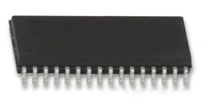
The THS1206 is a CMOS, low-power, 12-bit, 6 MSPS analog-to-digital converter (ADC). The speed, resolution, bandwidth, and single-supply operation are suited for applications in radar, imaging, high-speed acquisition, and communications. A multistage pipelined architecture with output error correction logic provides for no missing codes over the full operating temperature range. Internal control registers are used to program the ADC into the desired mode. The THS1206 consists of four analog inputs, which are sampled simultaneously. These inputs can be selected individually and configured to single-ended or differential inputs. An integrated 16 word deep FIFO allows the storage of data in order to take the load off of the processor connected to the ADC. Internal reference voltages for the ADC (1.5 V and 3.5 V) are provided. An external reference can also be chosen to suit the dc accuracy and temperature drift requirements of the application. Two different conversion modes can be selected. In single conversion mode, a single and simultaneous conversion of up to four inputs can be initiated by using the single conversion start signal (CONVST). The conversion clock in single conversion mode is generated internally using a clock oscillator circuit. In continuous conversion mode, an external clock signal is applied to the CONV_CLK input of the THS1206. The internal clock oscillator is switched off in continuous conversion mode. The THS1206C is characterized for operation from 0°C to 70°C, the THS1206I is characterized for operation from –40°C to 85°C, the THS1206Q is characterized to meet the rigorous requirements of the automotive environment from –40°C to 125°C, and the THS1206M is characterized for operation over the full military temperature range of –55°C to 125°C.
- Radar Applications
- Communications
- Control Applications
- High-Speed DSP Front-End
- Automotive Applications


