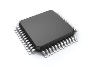
ADC Single 200Msps 8-bit Parallel 48-Pin TQFP Tray, ADC08B200CIVS/NOPB, Texas Instruments

The ADC08B200 is a high speed analog-to-digital converter (ADC) with an integrated capture buffer. The 8-bit, 200 MSPS A/D core is based upon the proven ADC08200 with integrated track-and-hold and is optimized for low power consumption. This device contains a selectable size capture buffer of up to 1,024 bytes that allows fast capture of an input signal with a slower readout rate. An on-chip clock PLL circuit provides the option of on-chip clock rate multiplication to provide the high speed sampling clock.The ADC08B200 is resistant to latch-up and the outputs are short-circuit proof. The top and bottom of the ADC08B200"s reference ladder are available for connections, enabling a wide range of input possibilities. The digital outputs are TTL/CMOS compatible with a separate output power supply pin to support interfacing with 2.7V to 3.3V logic. The digital inputs and outputs are low voltage TTL/CMOS compatible and the output data format is straight binary.The ADC08B200Q runs on an Automotive Grade Flow and is AEC-Q100 Grade 2 Qualified. The ADC08B200 is offered in a 48-pin plastic package (TQFP) and is specified over the extended industrial temperature range of -40°C to +105°C. An evaluation board is available to assist in the easy evaluation of the ADC08B200.

  • Single-Ended Input
  • Selectable Capture Buffer Size
  • PLL for Clock Multiplication
  • Reference Ladder Top and Bottom Accessible
  • Linear Power Scaling with Sample Rate
  • FPGA Training Pattern
  • AEC-Q100 Grade 2 Qualified
  • Power-Down Feature
  • (PLL Bypassed)

  • Resolution 8 Bits
  • Maximum Sampling Frequency 200 MSPS (min)
  • DNL ±0.4 LSB (typ)
  • ENOB (fIN= 49 MHz) 7.2 bits (typ)
  • THD (fIN= 49 MHz) -53 dBc (typ)
  • Power Consumption
    • Operating (50 MHz) Input 2 mW / Msps (typ)
    • Power Down 2.15 mW (typ)
  • Характеристики

    Volt_supply_source

    Analog and Digital

    Number_of_analog_inputs

    1

    Sampling_rate

    200 Msps

    Volt_reference

    External

    Digital_supply_support

    Yes

    Resolution

    8 Bit

    Differential_nonlinearity

    0.9 LSB

    Signal_to_noise_ratio

    47 dB

    Input_type

    Voltage

    Input_signal_type

    Single-Ended

    Input_volt

    1.6 V

    Бренд

    Msl_level

    3

    Country_of_origin

    Malaysia

    Eccn

    EAR99

    Htsn

    8542390001

    Lead_finish

    Matte Tin

    Max_processing_temp

    260

    Mounting

    Surface Mount

    Operating_temp

    -40 to 105 °C

    Pin_count

    48

    Product_dimensions

    7 x 7 x 1 mm

    Schedule_b

    8542390000

    Screening_level

    Extended Industrial

    Specifications

    http://www.ti.com/general/docs/lit/getliterature.tsp?genericPartNumber=ADC08B200&&fileType=pdf

    Supplier_package

    TQFP

    Polarity_of_input_volt

    Unipolar

    Operating_supply_volt

    3, 3.3 V, 3.6

    Number_of_adcs

    1

    Digital_interface_type

    Parallel

    Артикул: ADC08B200CIVS/NOPB

    Описание

    The ADC08B200 is a high speed analog-to-digital converter (ADC) with an integrated capture buffer. The 8-bit, 200 MSPS A/D core is based upon the proven ADC08200 with integrated track-and-hold and is optimized for low power consumption. This device contains a selectable size capture buffer of up to 1,024 bytes that allows fast capture of an input signal with a slower readout rate. An on-chip clock PLL circuit provides the option of on-chip clock rate multiplication to provide the high speed sampling clock.The ADC08B200 is resistant to latch-up and the outputs are short-circuit proof. The top and bottom of the ADC08B200"s reference ladder are available for connections, enabling a wide range of input possibilities. The digital outputs are TTL/CMOS compatible with a separate output power supply pin to support interfacing with 2.7V to 3.3V logic. The digital inputs and outputs are low voltage TTL/CMOS compatible and the output data format is straight binary.The ADC08B200Q runs on an Automotive Grade Flow and is AEC-Q100 Grade 2 Qualified. The ADC08B200 is offered in a 48-pin plastic package (TQFP) and is specified over the extended industrial temperature range of -40°C to +105°C. An evaluation board is available to assist in the easy evaluation of the ADC08B200.

  • Single-Ended Input
  • Selectable Capture Buffer Size
  • PLL for Clock Multiplication
  • Reference Ladder Top and Bottom Accessible
  • Linear Power Scaling with Sample Rate
  • FPGA Training Pattern
  • AEC-Q100 Grade 2 Qualified
  • Power-Down Feature
  • (PLL Bypassed)

  • Resolution 8 Bits
  • Maximum Sampling Frequency 200 MSPS (min)
  • DNL ±0.4 LSB (typ)
  • ENOB (fIN= 49 MHz) 7.2 bits (typ)
  • THD (fIN= 49 MHz) -53 dBc (typ)
  • Power Consumption
    • Operating (50 MHz) Input 2 mW / Msps (typ)
    • Power Down 2.15 mW (typ)
  • Детали

    Volt_supply_source

    Analog and Digital

    Number_of_analog_inputs

    1

    Sampling_rate

    200 Msps

    Volt_reference

    External

    Digital_supply_support

    Yes

    Resolution

    8 Bit

    Differential_nonlinearity

    0.9 LSB

    Signal_to_noise_ratio

    47 dB

    Input_type

    Voltage

    Input_signal_type

    Single-Ended

    Input_volt

    1.6 V

    Бренд

    Msl_level

    3

    Country_of_origin

    Malaysia

    Eccn

    EAR99

    Htsn

    8542390001

    Lead_finish

    Matte Tin

    Max_processing_temp

    260

    Mounting

    Surface Mount

    Operating_temp

    -40 to 105 °C

    Pin_count

    48

    Product_dimensions

    7 x 7 x 1 mm

    Schedule_b

    8542390000

    Screening_level

    Extended Industrial

    Specifications

    http://www.ti.com/general/docs/lit/getliterature.tsp?genericPartNumber=ADC08B200&&fileType=pdf

    Supplier_package

    TQFP

    Polarity_of_input_volt

    Unipolar

    Operating_supply_volt

    3, 3.3 V, 3.6

    Number_of_adcs

    1

    Digital_interface_type

    Parallel