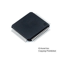
MCU 32-Bit PIC32MX3xx PIC RISC 64KB Flash 2.5V/3.3V 64-Pin TQFP T/R, PIC32MX430F064HT-V/PT, Microchip

PIC32MX430 is 32-bit Microcontrollers (up to 512 KB Flash and 128 KB SRAM) with Audio/Graphics/Touch (HMI), USB, and Advanced Analog P>The the MIPS32 M4K Processor Core is the heart of the PIC32MX330/350/370/430/450/470 device processor. The CPU fetches instructions, decodes each instruction, fetches source operands, executes each instruction and writes the results of instruction execution to the proper destinations The MIPS32 M4K processor core contains several logic blocks working together in parallel, providing an efficient high-performance computing engine. The following blocks are included with the core: Execution Unit Multiply/Divide Unit (MDU) System Control Coprocessor (CP0) Fixed Mapping Translation (FMT) Dual Internal Bus interfaces Power Management MIPS16e Support Enhanced JTAG (EJTAG) Controller The MIPS32 M4K processor core execution unit implements a load/store architecture with single-cycle ALU operations (logical, shift, add, subtract) and an autonomous multiply/divide unit. The core contains thirty-two 32-bit General Purpose Registers (GPRs) used for integer operations and address calculation. One additional register file shadow set (containing thirty-two registers) is added to minimize context switching overhead during interrupt/exception processing. The register file consists of two read ports and one write port and is fully bypassed to minimize operation latency in the pipeline. The execution unit includes: 32-bit adder used for calculating the data address Address unit for calculating the next instruction address Logic for branch determination and branch target address calculation Load aligner Bypass multiplexers used to avoid stalls when executing instruction streams where data producing instructions are followed closely by consumers of their results Leading Zero/One detect unit for implementing the CLZ and CLO instructions Arithmetic Logic Unit (ALU) for performing bitwise logical operations Shifter and store aligner The MIPS32 M4K processor core includes a Multiply/Divide Unit (MDU) that contains a separate pipeline for multiply and divide operations. This pipeline operates in parallel with the Integer Unit (IU) pipeline and does not stall when the IU pipeline stalls. This allows MDU operations to be partially masked by system stalls and/or other integer unit instructions The high-performance MDU consists of a 32×16 booth recoded multiplier, result/accumulation registers (HI and LO), a divide state machine, and the necessary multiplexers and control logic. The first number shown (‘32’ of 32×16) represents the rs operand. The second number (‘16’ of 32×16) represents the rt operand. The PIC32 core only checks the value of the latter (rt) operand to determine how many times the operation must pass through the multiplier. The 16×16 and 32×16 operations pass through the multiplier once. A 32×32 operation passes through the multiplier twice The MDU supports execution of one 16×16 or 32×16 multiply operation every clock cycle; 32×32 multiply operations can be issued every other clock cycle. Appropriate interlocks are implemented to stall the issuance of back-to-back 32×32 multiply operations. The multiply operand size is automatically determined by logic built into the MDU Divide operations are implemented with a simple 1 bit per clock iterative algorithm. An early-in detection checks the sign extension of the dividend (rs) operand. If rs is 8 bits wide, 23 iterations are skipped. For a 16-bit wide rs , 15 iterations are skipped and for a 24-bit wide rs, 7 iterations are skipped. Any attempt to issue a subsequent MDU instruction while a divide is still active causes an IU pipeline stall until the divide operation is completed

  • Core: 100 MHz/131 DMIPS MIPS32® M4K®
  • MIPS16e® mode for up to 40% smaller code size
  • Code-efficient (C and Assembly) architecture
  • Single-cycle (MAC) 32×16 and two-cycle 32×32 multiply
  • Clock Management
  • 0.9% internal oscillator
  • Programmable PLLs and oscillator clock sources
  • Fail-Safe Clock Monitor (FSCM)
  • Independent Watchdog Timer
  • Fast wake-up and start-up
  • Power Management
  • Low-power management modes (Sleep and Idle)
  • Integrated Power-on Reset, Brown-out Reset, and High
  • Voltage Detect
  • 0.5 mA/MHz dynamic current (typical)
  • 50µA IPD current (typical)
  • Audio/Graphics/Touch HMI Features
  • External graphics interface with up to 34 PMP pins
  • Audio data communication: I2S, LJ, RJ, USB
  • Audio data control interface: SPI and I2C™
  • Audio data master clock:
    • Generation of fractional clock frequencies
    • Can be synchronized with USB clock
    • Can be tuned in run-time
  • Charge Time Measurement Unit (CTMU):
    • Supports mTouch™ capacitive touch sensing
    • Provides high-resolution time measurement (1 ns) Advanced Analog Features
  • ADC Module:
    • 10-bit 1 Msps rate with one Sample and Hold (S&H)
    • Up to 28 analog inputs
    • Can operate during Sleep mode
  • Flexible and independent ADC trigger sources
  • On-chip temperature measurement capability
  • Comparators:
    • Two dual-input Comparator modules
    • Programmable references with 32 voltage points Timers/Output Compare/Input Capture
  • Five General Purpose Timers:
    • Five 16-bit and up to two 32-bit Timers/Counters
  • Five Output Compare (OC) modules
  • Five Input Capture (IC) modules
  • Peripheral Pin Select (PPS) to allow function remap
  • Real-Time Clock and Calendar (RTCC) module
  • Communication Interfaces
  • USB 2.0-compliant Full-speed OTG controller
  • Up to five UART modules (20 Mbps):
    • LIN 1.2 protocols and IrDA®support
  • Two 4-wire SPI modules (25 Mbps)
  • Two I2C modules (up to 1 Mbaud) with SMBus support
  • PPS to allow function remap
  • Parallel Master Port (PMP)
  • Direct Memory Access (DMA)
  • Four channels of hardware DMA with automatic data size detection
  • 32-bit Programmable Cyclic Redundancy Check (CRC)
  • Two additional channels dedicated to USB
  • Input/Output
  • 15 mA or 12 mA source/sink for standard VOH/VOL and up to 22 mA for non-standard VOH1
  • 5V-tolerant pins
  • Selectable open drain, pull-ups, and pull-downs
  • External interrupts on all I/O pins Qualification and Class B Support
  • AEC-Q100 REVG (Grade 2 -40°C to +105°C) planned
  • Class B Safety Library, IEC 60730
  • Debugger Development Support
  • In-circuit and in-application programming
  • 4-wire MIPS®
  • Enhanced JTAG interface
  • Unlimited program and six complex data breakpoints
  • IEEE 1149.2-compatible (JTAG) boundary scan
Характеристики

Analog_comparators

2

Specifications

https://4donline.ihs.com/images/VipMasterIC/IC/MCHP/MCHP-S-A0003513816/MCHP-S-A0003513816-1.pdf?hkey=52A5661711E402568146F3353EA87419

Number_of_programmable_i_os

49

Number_of_timers

5

On_chip_adc

28-chx10-bit

Operating_supply_voltage

2.5, 3.3 V

Operating_temperature

-40 to 105 °C

Pin_count

64

Product_dimensions

10 x 10 x 1 mm

Program_memory_type

Flash

Mounting

Surface Mount

Ram_size

16 Kb

Schedule_b

8542310000

Screening_level

Automotive

Special_features

LCD Controller

Program_memory_size

8 KB

Watchdog

1

Supplier_package

TQFP

Min_operating_supply_voltage

2.3 V

Бренд

Country_of_origin

Thailand

Data_bus_width

32 Bit

Device_core

PIC

Eccn

3A991.A.2

Htsn

8542310001

Max_speed

80 MHz

Instruction_set_architecture

RISC

Тип интерфейса

I2C/JTAG/I2S/SPI/UART/USB

Lcd_segments

8192

Lead_finish

Matte Tin

Max_operating_supply_voltage

3.6 V

Max_processing_temp

260 °C

Артикул: PIC32MX430F064HT-V/PT

Описание

PIC32MX430 is 32-bit Microcontrollers (up to 512 KB Flash and 128 KB SRAM) with Audio/Graphics/Touch (HMI), USB, and Advanced Analog P>The the MIPS32 M4K Processor Core is the heart of the PIC32MX330/350/370/430/450/470 device processor. The CPU fetches instructions, decodes each instruction, fetches source operands, executes each instruction and writes the results of instruction execution to the proper destinations The MIPS32 M4K processor core contains several logic blocks working together in parallel, providing an efficient high-performance computing engine. The following blocks are included with the core: Execution Unit Multiply/Divide Unit (MDU) System Control Coprocessor (CP0) Fixed Mapping Translation (FMT) Dual Internal Bus interfaces Power Management MIPS16e Support Enhanced JTAG (EJTAG) Controller The MIPS32 M4K processor core execution unit implements a load/store architecture with single-cycle ALU operations (logical, shift, add, subtract) and an autonomous multiply/divide unit. The core contains thirty-two 32-bit General Purpose Registers (GPRs) used for integer operations and address calculation. One additional register file shadow set (containing thirty-two registers) is added to minimize context switching overhead during interrupt/exception processing. The register file consists of two read ports and one write port and is fully bypassed to minimize operation latency in the pipeline. The execution unit includes: 32-bit adder used for calculating the data address Address unit for calculating the next instruction address Logic for branch determination and branch target address calculation Load aligner Bypass multiplexers used to avoid stalls when executing instruction streams where data producing instructions are followed closely by consumers of their results Leading Zero/One detect unit for implementing the CLZ and CLO instructions Arithmetic Logic Unit (ALU) for performing bitwise logical operations Shifter and store aligner The MIPS32 M4K processor core includes a Multiply/Divide Unit (MDU) that contains a separate pipeline for multiply and divide operations. This pipeline operates in parallel with the Integer Unit (IU) pipeline and does not stall when the IU pipeline stalls. This allows MDU operations to be partially masked by system stalls and/or other integer unit instructions The high-performance MDU consists of a 32×16 booth recoded multiplier, result/accumulation registers (HI and LO), a divide state machine, and the necessary multiplexers and control logic. The first number shown (‘32’ of 32×16) represents the rs operand. The second number (‘16’ of 32×16) represents the rt operand. The PIC32 core only checks the value of the latter (rt) operand to determine how many times the operation must pass through the multiplier. The 16×16 and 32×16 operations pass through the multiplier once. A 32×32 operation passes through the multiplier twice The MDU supports execution of one 16×16 or 32×16 multiply operation every clock cycle; 32×32 multiply operations can be issued every other clock cycle. Appropriate interlocks are implemented to stall the issuance of back-to-back 32×32 multiply operations. The multiply operand size is automatically determined by logic built into the MDU Divide operations are implemented with a simple 1 bit per clock iterative algorithm. An early-in detection checks the sign extension of the dividend (rs) operand. If rs is 8 bits wide, 23 iterations are skipped. For a 16-bit wide rs , 15 iterations are skipped and for a 24-bit wide rs, 7 iterations are skipped. Any attempt to issue a subsequent MDU instruction while a divide is still active causes an IU pipeline stall until the divide operation is completed

  • Core: 100 MHz/131 DMIPS MIPS32® M4K®
  • MIPS16e® mode for up to 40% smaller code size
  • Code-efficient (C and Assembly) architecture
  • Single-cycle (MAC) 32×16 and two-cycle 32×32 multiply
  • Clock Management
  • 0.9% internal oscillator
  • Programmable PLLs and oscillator clock sources
  • Fail-Safe Clock Monitor (FSCM)
  • Independent Watchdog Timer
  • Fast wake-up and start-up
  • Power Management
  • Low-power management modes (Sleep and Idle)
  • Integrated Power-on Reset, Brown-out Reset, and High
  • Voltage Detect
  • 0.5 mA/MHz dynamic current (typical)
  • 50µA IPD current (typical)
  • Audio/Graphics/Touch HMI Features
  • External graphics interface with up to 34 PMP pins
  • Audio data communication: I2S, LJ, RJ, USB
  • Audio data control interface: SPI and I2C™
  • Audio data master clock:
    • Generation of fractional clock frequencies
    • Can be synchronized with USB clock
    • Can be tuned in run-time
  • Charge Time Measurement Unit (CTMU):
    • Supports mTouch™ capacitive touch sensing
    • Provides high-resolution time measurement (1 ns) Advanced Analog Features
  • ADC Module:
    • 10-bit 1 Msps rate with one Sample and Hold (S&H)
    • Up to 28 analog inputs
    • Can operate during Sleep mode
  • Flexible and independent ADC trigger sources
  • On-chip temperature measurement capability
  • Comparators:
    • Two dual-input Comparator modules
    • Programmable references with 32 voltage points Timers/Output Compare/Input Capture
  • Five General Purpose Timers:
    • Five 16-bit and up to two 32-bit Timers/Counters
  • Five Output Compare (OC) modules
  • Five Input Capture (IC) modules
  • Peripheral Pin Select (PPS) to allow function remap
  • Real-Time Clock and Calendar (RTCC) module
  • Communication Interfaces
  • USB 2.0-compliant Full-speed OTG controller
  • Up to five UART modules (20 Mbps):
    • LIN 1.2 protocols and IrDA®support
  • Two 4-wire SPI modules (25 Mbps)
  • Two I2C modules (up to 1 Mbaud) with SMBus support
  • PPS to allow function remap
  • Parallel Master Port (PMP)
  • Direct Memory Access (DMA)
  • Four channels of hardware DMA with automatic data size detection
  • 32-bit Programmable Cyclic Redundancy Check (CRC)
  • Two additional channels dedicated to USB
  • Input/Output
  • 15 mA or 12 mA source/sink for standard VOH/VOL and up to 22 mA for non-standard VOH1
  • 5V-tolerant pins
  • Selectable open drain, pull-ups, and pull-downs
  • External interrupts on all I/O pins Qualification and Class B Support
  • AEC-Q100 REVG (Grade 2 -40°C to +105°C) planned
  • Class B Safety Library, IEC 60730
  • Debugger Development Support
  • In-circuit and in-application programming
  • 4-wire MIPS®
  • Enhanced JTAG interface
  • Unlimited program and six complex data breakpoints
  • IEEE 1149.2-compatible (JTAG) boundary scan
Детали

Analog_comparators

2

Specifications

https://4donline.ihs.com/images/VipMasterIC/IC/MCHP/MCHP-S-A0003513816/MCHP-S-A0003513816-1.pdf?hkey=52A5661711E402568146F3353EA87419

Number_of_programmable_i_os

49

Number_of_timers

5

On_chip_adc

28-chx10-bit

Operating_supply_voltage

2.5, 3.3 V

Operating_temperature

-40 to 105 °C

Pin_count

64

Product_dimensions

10 x 10 x 1 mm

Program_memory_type

Flash

Mounting

Surface Mount

Ram_size

16 Kb

Schedule_b

8542310000

Screening_level

Automotive

Special_features

LCD Controller

Program_memory_size

8 KB

Watchdog

1

Supplier_package

TQFP

Min_operating_supply_voltage

2.3 V

Бренд

Country_of_origin

Thailand

Data_bus_width

32 Bit

Device_core

PIC

Eccn

3A991.A.2

Htsn

8542310001

Max_speed

80 MHz

Instruction_set_architecture

RISC

Тип интерфейса

I2C/JTAG/I2S/SPI/UART/USB

Lcd_segments

8192

Lead_finish

Matte Tin

Max_operating_supply_voltage

3.6 V

Max_processing_temp

260 °C