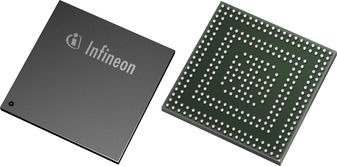
Описание
The TC1197 combines three powerful technologies within one silicon die, achieving new levels of power, speed, and economy for embedded applications: Reduced Instruction Set Computing (RISC) processor architectureDigital Signal Processing (DSP) operations and addressing modesOn-chip memories and peripherals DSP operations and addressing modes provide the computational power necessary to efficiently analyze complex real-world signals. The RISC load/store architecture provides high computational bandwidth with low system cost. On-chip memory and peripherals are designed to support even the most demanding high-bandwidth real-time embedded control-systems tasks. The TC1197 is a high-performance microcontroller with TriCore CPU, program and data memories, buses, bus arbitration, an interrupt controller, a peripheral control processor and a DMA controller and several on-chip peripherals. The TC1197 is designed to meet the needs of the most demanding embedded control systems applications where the competing issues of price/performance, real-time responsiveness, computational power, data bandwidth, and power consumption are key design elements. The TC1197 offers several versatile on-chip peripheral units such as serial controllers, timer units, and Analog-to-Digital converters. Within the TC1197, all these peripheral units are connected to the TriCore CPU/system via the Flexible Peripheral Interconnect (FPI) Bus and the Local Memory Bus (LMB). Several I/O lines on the TC1197 ports are reserved for these peripheral units to communicate with the external world.
- High-performance 32-bit super-scalar TriCore V1.3.1 CPU with 4-stage pipeline
- Superior real-time performance
- Strong bit handling
- Fully integrated DSP capabilities
- Single precision Floating Point Unit (FPU)
- 180 MHz operation at full temperature range
- 32-bit Peripheral Control Processor with single cycle instruction (PCP2)
- 16 Kbyte Parameter Memory (PRAM)
- 32 Kbyte Code Memory (CMEM)
- 180 MHz operation at full temperature range
- Multiple on-chip memories
- 4 or 2 Mbyte Program Flash Memory (PFLASH) with ECC
- 64 Kbyte Data Flash Memory (DFLASH) usable for EEPROM emulation
- 128 Kbyte Data Memory (LDRAM)
- 40 Kbyte Code Scratchpad Memory (SPRAM)
- Instruction Cache: up to 16 Kbyte (ICACHE, configurable)
- Data Cache: up to 4 Kbyte (DCACHE, configurable)
- 8 Kbyte Overlay Memory (OVRAM)
- 16 Kbyte BootROM (BROM)
- 16-Channel DMA Controller
- 32-bit External Bus Interface Unit (EBU) with
- 32-bit demultiplexed / 16-bit multiplexed external bus interface (3.3V, 2.5V)
- Support for Burst Flash memory devices
- Scalable external bus timing up to 75 MHz
- Sophisticated interrupt system with 2 × 255 hardware priority arbitration levels serviced by CPU or PCP2
- High performing on-chip bus structure
- 64-bit Local Memory Buses between CPU, EBU, Flash and Data Memory
- 32-bit System Peripheral Bus (SPB) for on-chip peripheral and functional units
- One bus bridges (LFI Bridge)
- Versatile On-chip Peripheral Units
- Two Asynchronous/Synchronous Serial Channels (ASC) with baud rate generator, parity, framing and overrun error detection
- Two High-Speed Synchronous Serial Channels (SSC) with programmable data length and shift direction
- Two serial Micro Second Bus interface (MSC) for serial port expansion to external power devices
- Two High-Speed Micro Link interface (MLI) for serial inter-processor communication
- One MultiCAN Module with 4 CAN nodes and 128 free assignable message objects for high efficiency data handling via FIFO buffering and gateway data transfer
- Two General Purpose Timer Array Modules (GPTA) with additional Local Timer Cell Array (LTCA2) providing a powerful set of digital signal filtering and timer functionality to realize autonomous and complex Input/Output management
- 44 analog input lines for ADC
- 3 independent kernels (ADC0, ADC1, ADC2)
- Analog supply voltage range from 3.3 V to 5 V (single supply)
- Performance for 12 bit resolution (@fADCI = 10 MHz)
- 4 different FADC input channels
- channels with impedance control and overlaid with ADC1 inputs
- Extreme fast conversion, 21 cycles of fFADC clock (262.5 ns @ fFADC = 80 MHz)
- 10-bit A/D conversion (higher resolution can be achieved by averaging of consecutive conversions in digital data reduction filter)
- 221 digital general purpose I/O lines1) (GPIO), 4 input lines
- Digital I/O ports with 3.3 V capability
- On-chip debug support for OCDS Level 1 (CPU, PCP, DMA, On Chip Bus)
- Dedicated Emulation Device chip available (TC1797ED)
- multi-core debugging, real time tracing, and calibration
- four/five wire JTAG (IEEE 1149.1) or two wire DAP (Device Access Port) interface
- Power Management System
- Clock Generation Unit with PLL
- Core supply voltage of 1.5 V
- I/O voltage of 3.3 V
- Temperature range: -40° to +125°C
- Package variants: PG-BGA-416-10