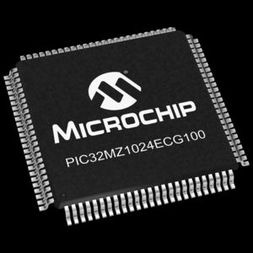
MCU 32-Bit PIC32 PIC RISC 1024KB Flash 3.3V 100-Pin TQFP, PIC32MZ1024ECG100-I/PT, Microchip

Microchip"s PIC32MZ1024ECG100 32-bit Microcontrollers provide class-leading performance of 330 DMIPS and 3.28 CoreMarks/MHz, along with dual-panel, live-update Flash (up to 2MB), large RAM (512KB) and the connectivity peripherals—including a 10/100 Ethernet MAC, Hi-Speed USB MAC/PHY (a first for PIC MCUs) and dual CAN ports—needed to support today"s demanding applications. The PIC32MZ also has class-leading code density that is 30% better than competitors, along with a 28Msps ADC that offers one of the best throughput rates for 32-bit MCUs. Rounding out this family"s high level of integration is a full-featured hardware crypto engine with a random number generator for high-throughput data encryption/decryption and authentication (e.g., AES, 3DES, SHA, MD5 and HMAC), as well as the first SQI interface on a Microchip MCU and the PIC32"s highest number of serial channels. The MIPS32 microAptiv Microprocessor Core is the heart of the PIC32MZ EC family device processor. The CPU fetches instructions, decodes each instruction, fetches source operands, executes each instruction and writes the results of instruction execution to the proper destinations. The MIPS32 microAptiv Microprocessor core in PIC32MZ EC family devices contains several logic blocks working together in parallel, providing an efficient high-performance computing engine. The following blocks are included with the core: Execution unit General Purpose Register (GPR) Multiply/Divide Unit (MDU) System control coprocessor (CP0) Memory Management Unit (MMU) Instruction/Data cache controllers Power Management Instructions and data caches microMIPS support Enhanced JTAG (EJTAG) controller The processor core execution unit implements a load/store architecture with single-cycle ALU operations (logical, shift, add, subtract) and an autonomous multiply/divide unit. The core contains thirty-two 32-bit General Purpose Registers (GPRs) used for integer operations and address calculation. Seven additional register file shadow sets (containing thirty-two registers) are added to minimize context switching overhead during interrupt/exception processing. The register file consists of two read ports and one write port and is fully bypassed to minimize operation latency in the pipeline.

  • Core: 200 MHz (up to 330 DMIPS) microAptiv™
  • 16 KB I-Cache, 4 KB D-Cache
  • MMU for optimum embedded OS execution
  • microMIPS™ mode for up to 35% smaller code size
  • DSP-enhanced core: – Four 64-bit accumulators – Single-cycle MAC, saturating and fractional math
  • Code-efficient (C and Assembly) architecture Clock Management
  • 0.9% internal oscillator
  • Programmable PLLs and oscillator clock sources
  • Fail-Safe Clock Monitor (FSCM)
  • Independent Watchdog Timers (WDT) and Deadman Timer (DMT)
  • Fast wake-up and start-up
  • Power Management
  • Low-power modes (Sleep and Idle)
  • Integrated Power-on Reset and Brown-out Reset
  • Memory Interfaces
  • 50 MHz External Bus Interface (EBI)
  • 50 MHz Serial Quad Interface (SQI) Audio and Graphics Interfaces
  • Graphics interfaces: EBI or PMP
  • Audio data communication: I2S, LJ, and RJ
  • Audio control interfaces: SPI and I2 C™
  • Audio master clock: Fractional clock frequencies with USB synchronization
  • High-Speed (HS) Communication Interfaces (with Dedicated DMA)
  • USB 2.0-compliant Hi-Speed On-The-Go (OTG) controller
  • 10/100 Mbps Ethernet MAC with MII and RMII interface Security Features
  • Crypto Engine with a RNG for data encryption/decryption and authentication (AES, 3DES, SHA, MD5, and HMAC)
  • Advanced memory protection: – Peripheral and memory region access control
  • Direct Memory Access (DMA)
  • Eight channels with automatic data size detection
  • Programmable Cyclic Redundancy Check (CRC)
  • Advanced Analog Features
  • 10-bit ADC resolution and up to 48 analog inputs
  • Flexible and independent ADC trigger sources
  • Two comparators with 32 programmable voltage references
  • Temperature sensor with ±2°C accuracy
  • Communication Interfaces
  • Two CAN modules (with dedicated DMA channels): – 2.0B Active with DeviceNet™ addressing support
  • Six UART modules (25 Mbps): – Supports LIN 1.2 and IrDA® protocols
  • Six 4-wire SPI modules
  • SQI configurable as an additional SPI module (50 MHz)
  • Five I2 C modules (up to 1 Mbaud) with SMBus support
  • Parallel Master Port (PMP)
  • Peripheral Pin Select (PPS) to enable function remap
  • Timers/Output Compare/Input Capture
  • Nine 16-bit or up to four 32-bit timers/counters
  • Nine Output Compare (OC) modules
  • Nine Input Capture (IC) modules
  • PPS to enable function remap
  • Real-Time Clock and Calendar (RTCC) module Input/Output
  • 5V-tolerant pins with up to 32 mA source/sink
  • Selectable open drain, pull-ups, and pull-downs
  • External interrupts on all I/O pins
  • Qualification and Class B Support
  • AEC-Q100 REVG (Grade 2 -40°C to +105°C) Planned
  • AEC-Q100 REVG (Grade 1 -40°C to +125°C) Planned
  • Class B Safety Library, IEC 60730
  • Back-up internal oscillator
  • Debugger Development Support
  • In-circuit and in-application programming
  • 4-wire MIPS® Enhanced JTAG interface
  • Unlimited software and 12 complex breakpoints
  • IEEE 1149.2-compatible (JTAG) boundary scan
  • Non-intrusive hardware-based instruction trace
  • Software and Tools Support
  • C/C++ compiler with native DSP/fractional support
  • MPLAB® Harmony Integrated Software Framework
  • TCP/IP, USB, Graphics, and mTouch™ middleware
  • MFi, Android™, and Bluetooth® audio frameworks
  • FreeRTOS™, OPENRTOS® , µC/OS™, and other popular RTOS kernels
Характеристики

Analog_comparators

2

Program_memory_size

1024 KB

Number_of_programmable_i_os

78

Number_of_timers

9

On_chip_adc

40-chx12-bit

Operating_supply_voltage

3.3 V

Operating_temperature

-40 to 85 °C

Pin_count

100

Product_dimensions

12 x 12 x 1

Program_memory_type

Flash

Mounting

Surface Mount

Ram_size

512 KB

Schedule_b

8542310000

Screening_level

Industrial

Specifications

https://4donline.ihs.com/images/VipMasterIC/IC/MCHP/MCHP-S-A0002750777/MCHP-S-A0002750777-1.pdf?hkey=52A5661711E402568146F3353EA87419

Supplier_package

TQFP

Watchdog

1

Msl_level

3

Min_operating_supply_voltage

2.2 V

Бренд

Country_of_origin

Thailand

Data_bus_width

32 Bit

Device_core

PIC

Eccn

3A991.A.2

Htsn

8542310001

Max_speed

200 MHz

Instruction_set_architecture

RISC

Тип интерфейса

I2C/I2S/SPI/UART/USB

Lead_finish

Matte Tin

Max_operating_supply_voltage

3.6 V

Max_processing_temp

260 °C

Артикул: PIC32MZ1024ECG100-I/PT

Описание

Microchip"s PIC32MZ1024ECG100 32-bit Microcontrollers provide class-leading performance of 330 DMIPS and 3.28 CoreMarks/MHz, along with dual-panel, live-update Flash (up to 2MB), large RAM (512KB) and the connectivity peripherals—including a 10/100 Ethernet MAC, Hi-Speed USB MAC/PHY (a first for PIC MCUs) and dual CAN ports—needed to support today"s demanding applications. The PIC32MZ also has class-leading code density that is 30% better than competitors, along with a 28Msps ADC that offers one of the best throughput rates for 32-bit MCUs. Rounding out this family"s high level of integration is a full-featured hardware crypto engine with a random number generator for high-throughput data encryption/decryption and authentication (e.g., AES, 3DES, SHA, MD5 and HMAC), as well as the first SQI interface on a Microchip MCU and the PIC32"s highest number of serial channels. The MIPS32 microAptiv Microprocessor Core is the heart of the PIC32MZ EC family device processor. The CPU fetches instructions, decodes each instruction, fetches source operands, executes each instruction and writes the results of instruction execution to the proper destinations. The MIPS32 microAptiv Microprocessor core in PIC32MZ EC family devices contains several logic blocks working together in parallel, providing an efficient high-performance computing engine. The following blocks are included with the core: Execution unit General Purpose Register (GPR) Multiply/Divide Unit (MDU) System control coprocessor (CP0) Memory Management Unit (MMU) Instruction/Data cache controllers Power Management Instructions and data caches microMIPS support Enhanced JTAG (EJTAG) controller The processor core execution unit implements a load/store architecture with single-cycle ALU operations (logical, shift, add, subtract) and an autonomous multiply/divide unit. The core contains thirty-two 32-bit General Purpose Registers (GPRs) used for integer operations and address calculation. Seven additional register file shadow sets (containing thirty-two registers) are added to minimize context switching overhead during interrupt/exception processing. The register file consists of two read ports and one write port and is fully bypassed to minimize operation latency in the pipeline.

  • Core: 200 MHz (up to 330 DMIPS) microAptiv™
  • 16 KB I-Cache, 4 KB D-Cache
  • MMU for optimum embedded OS execution
  • microMIPS™ mode for up to 35% smaller code size
  • DSP-enhanced core: – Four 64-bit accumulators – Single-cycle MAC, saturating and fractional math
  • Code-efficient (C and Assembly) architecture Clock Management
  • 0.9% internal oscillator
  • Programmable PLLs and oscillator clock sources
  • Fail-Safe Clock Monitor (FSCM)
  • Independent Watchdog Timers (WDT) and Deadman Timer (DMT)
  • Fast wake-up and start-up
  • Power Management
  • Low-power modes (Sleep and Idle)
  • Integrated Power-on Reset and Brown-out Reset
  • Memory Interfaces
  • 50 MHz External Bus Interface (EBI)
  • 50 MHz Serial Quad Interface (SQI) Audio and Graphics Interfaces
  • Graphics interfaces: EBI or PMP
  • Audio data communication: I2S, LJ, and RJ
  • Audio control interfaces: SPI and I2 C™
  • Audio master clock: Fractional clock frequencies with USB synchronization
  • High-Speed (HS) Communication Interfaces (with Dedicated DMA)
  • USB 2.0-compliant Hi-Speed On-The-Go (OTG) controller
  • 10/100 Mbps Ethernet MAC with MII and RMII interface Security Features
  • Crypto Engine with a RNG for data encryption/decryption and authentication (AES, 3DES, SHA, MD5, and HMAC)
  • Advanced memory protection: – Peripheral and memory region access control
  • Direct Memory Access (DMA)
  • Eight channels with automatic data size detection
  • Programmable Cyclic Redundancy Check (CRC)
  • Advanced Analog Features
  • 10-bit ADC resolution and up to 48 analog inputs
  • Flexible and independent ADC trigger sources
  • Two comparators with 32 programmable voltage references
  • Temperature sensor with ±2°C accuracy
  • Communication Interfaces
  • Two CAN modules (with dedicated DMA channels): – 2.0B Active with DeviceNet™ addressing support
  • Six UART modules (25 Mbps): – Supports LIN 1.2 and IrDA® protocols
  • Six 4-wire SPI modules
  • SQI configurable as an additional SPI module (50 MHz)
  • Five I2 C modules (up to 1 Mbaud) with SMBus support
  • Parallel Master Port (PMP)
  • Peripheral Pin Select (PPS) to enable function remap
  • Timers/Output Compare/Input Capture
  • Nine 16-bit or up to four 32-bit timers/counters
  • Nine Output Compare (OC) modules
  • Nine Input Capture (IC) modules
  • PPS to enable function remap
  • Real-Time Clock and Calendar (RTCC) module Input/Output
  • 5V-tolerant pins with up to 32 mA source/sink
  • Selectable open drain, pull-ups, and pull-downs
  • External interrupts on all I/O pins
  • Qualification and Class B Support
  • AEC-Q100 REVG (Grade 2 -40°C to +105°C) Planned
  • AEC-Q100 REVG (Grade 1 -40°C to +125°C) Planned
  • Class B Safety Library, IEC 60730
  • Back-up internal oscillator
  • Debugger Development Support
  • In-circuit and in-application programming
  • 4-wire MIPS® Enhanced JTAG interface
  • Unlimited software and 12 complex breakpoints
  • IEEE 1149.2-compatible (JTAG) boundary scan
  • Non-intrusive hardware-based instruction trace
  • Software and Tools Support
  • C/C++ compiler with native DSP/fractional support
  • MPLAB® Harmony Integrated Software Framework
  • TCP/IP, USB, Graphics, and mTouch™ middleware
  • MFi, Android™, and Bluetooth® audio frameworks
  • FreeRTOS™, OPENRTOS® , µC/OS™, and other popular RTOS kernels

Детали

Analog_comparators

2

Program_memory_size

1024 KB

Number_of_programmable_i_os

78

Number_of_timers

9

On_chip_adc

40-chx12-bit

Operating_supply_voltage

3.3 V

Operating_temperature

-40 to 85 °C

Pin_count

100

Product_dimensions

12 x 12 x 1

Program_memory_type

Flash

Mounting

Surface Mount

Ram_size

512 KB

Schedule_b

8542310000

Screening_level

Industrial

Specifications

https://4donline.ihs.com/images/VipMasterIC/IC/MCHP/MCHP-S-A0002750777/MCHP-S-A0002750777-1.pdf?hkey=52A5661711E402568146F3353EA87419

Supplier_package

TQFP

Watchdog

1

Msl_level

3

Min_operating_supply_voltage

2.2 V

Бренд

Country_of_origin

Thailand

Data_bus_width

32 Bit

Device_core

PIC

Eccn

3A991.A.2

Htsn

8542310001

Max_speed

200 MHz

Instruction_set_architecture

RISC

Тип интерфейса

I2C/I2S/SPI/UART/USB

Lead_finish

Matte Tin

Max_operating_supply_voltage

3.6 V

Max_processing_temp

260 °C