Описание
The V850ES/JG3-L is a 32-bit single-chip microcontroller that includes the V850ES CPU core and peripheral functions such as ROM/RAM, timer/counters, serial interfaces, an A/D converter, and a D/A converter.In addition to high real-time response characteristics and 1-clock-pitch basic instructions, the V850ES/JG3-L features multiply instructions, saturated operation instructions, bit manipulation instructions, etc., realized by a hardware multiplier, as optimum instructions for digital servo control applications. Moreover, as a real-time control system, the V850ES/JG3-L enables an extremely high cost-performance for applications that require super low power consumption, such as digital cameras, electrical power meters, and mobile terminals.
- Minimum instruction execution time: 50 ns (operating on main clock (fXX) of 20 MHz: VDD = 2.7 to 3.6 V)
- 200 ns (operating on main clock (fXX) of 5 MHz: VDD = 2.2 to 3.6 V)
- 400 ns (operating on main clock (fXX) of 2.5 MHz: VDD = 2.0 to 3.6 V)
- 30.5µs (operating on sub clock (fXT) of 32.768 kHz)
- µPD70F3792, 70F3793, 70F3841, 70F3842 only
- General-purpose registers: 32 bits x 32 registers
- CPU features: Signed multiplication (16 x 16 x 32): 1 to 2 clocks
- Signed multiplication (32 x 32 x 64): 1 to 5 clocks
- Saturated operations (overflow and underflow detection functions included)
- Most instructions can be executed in 1 clock cycle by using 32-bit RISC-based 5-stage pipeline architecture
- Instruction fetching from internal ROM and accessing internal RAM for data can be executed separately, by using Harvard architecture
- High code efficiency achieved by using variable length instructions
- 32-bit shift instruction: 1 clock cycle
- Bit manipulation instructions
- Load/store instructions with long/short format
- Memory space: 64 MB of linear address space (for programs and data)
- External expansion: Up to 16 MB (including 1 MB used as internal ROM/RAM)
- Internal memory: RAM: 8/16/32/40 /80 KB
- Flash memory: 128 K/256 K/384 K/512 K/768 K/1 MB
- External bus interface: Separate bus/multiplexed bus output selectable(? PD70F3737, 70F3738,70F3792, 70F3793)
- Multiplexed bus mode (PD70F3841, 70F3842)
- 8/16 bit data bus sizing function
- Wait function
- Programmable wait function
- External wait function
- Idle state function
- Bus hold function
- Ports: I/O ports: 84 (µPD70F3737, 70F3738)
- 83 (µPD70F3792, 70F3793, 70F3841, 70F3842)
- Timer function: 16-bit interval timer M (TMM): 1 channel
- 16-bit timer/event counter P (TMP): 6 channels
- 16-bit timer/event counter Q (TMQ): 1 channel
- Watch timer: 1 channel
- Watchdog timer: 1 channel
- Real-time counter : 1 channel
- Real-time output port: 6 bits x 1 channel
- Serial interface: Asynchronous serial interface A (UARTA)
- 3-wire variable-length serial interface B (CSIB)
- I2C bus interface (I2C)
- UARTA/CSIB: 1 channel
- UARTA/I2C: 2 channels
- CSIB/I2C: 1 channel
- CSIB: 3 channels
- UARTA : 3 channels
- UARTCNote: 1 channel
- A/D converter: 10-bit resolution: 12 channels
- D/A converter: 8-bit resolution: 2 channels
- DMA controller: 4 channels
- DCU (debug control unit): JTAG interface
- Clock generator: During main clock or sub clock operation
- 7-level CPU clock (fXX, fXX/2, fXX/4, fXX/8, fXX/16, fXX/32, fXT)
- Clock-through mode/PLL mode selectable
- Internal oscillator clock: 220 kHz (TYP.)
- Power-save functions: HALT/IDLE1/IDLE2/STOP/low-voltage STOP/sub clock/sub-IDLE/
- low-voltage sub clock/low-voltage sub-IDLE mode (/RTC backup mode)
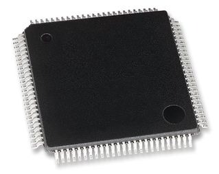
- Package: 100-pin plastic LQFP (fine pitch) (14 x 14)
- 121-pin plastic FBGA (8 x 8)
- Power supply voltage: VDD = 2.0 V to 3.6 V (2.5 MHz)
- VDD = 2.2 V to 3.6 V (5 MHz)
- VDD = 2.7 V to 3.6 V (20 MHz)