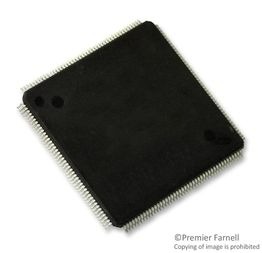
MCU 32-bit SPC564A80x e200 RISC 4096KB Flash 1.2V/3.3V/5V 176-Pin LQFP T/R, SPC564A80L7CFBR, STMicroelectronics

The microcontroller’s e200z4 host processor core is built on Power Architecture technology and designed specifically for embedded applications. In addition to the Power Architecture technology, this core supports instructions for digital signal processing (DSP).

  • 150 MHz e200z4 Power Architecture core
  • Variable length instruction encoding (VLE)
  • Superscalar architecture with 2 execution units
  • Up to 2 integer or floating point instructions per cycle
  • Up to 4 multiply and accumulate operations per cycle
  • Memory organization
  • 4 MB on-chip flash memory with ECC and Read While Write (RWW)
  • 192 KB on-chip RAM with standby functionality (32 KB) and ECC
  • 8 KB instruction cache (with line locking), configurable as 2- or 4-way
  • 14 + 3 KB eTPU code and data RAM
  • 5 × 4 crossbar switch (XBAR)
  • 24-entry MMU
  • External Bus Interface (EBI) with slave and master port
  • Fail Safe Protection
  • 16-entry Memory Protection Unit (MPU)
  • CRC unit with 3 sub-modules
  • Junction temperature sensor
  • Interrupts
  • Configurable interrupt controller (with NMI)
  • 64-channel DMA
  • Serial channels
  • 3 × eSCI
  • 3 × DSPI (2 of which support downstream Micro Second Channel [MSC])
  • 3 × FlexCAN with 64 messages each
  • 1 × FlexRay module (V2.1) up to 10 Mbit/s with dual or single channel and 128 message objects and ECC
  • 1 × eMIOS
  • 24 unified channels
  • 1 × eTPU2 (second generation eTPU)
  • 32 standard channels
  • 1 × reaction module (6 channels with three outputs per channel)
  • 2 enhanced queued analog-to-digital converters (eQADCs)
  • Forty 12-bit input channels (multiplexed on 2 ADCs); expandable to 56 channels with external multiplexers
  • 6 command queues
  • Trigger and DMA support
  • 688 ns minimum conversion time
  • On-chip CAN/SCI/FlexRay Bootstrap loader with Boot Assist Module (BAM)
  • Nexus: Class 3+ for core; Class 1 for the eTPU
  • JTAG (5-pin)
  • Development Trigger Semaphore (DTS)
  • Clock generation
  • On-chip 4–40 MHz main oscillator
  • On-chip FMPLL (frequency-modulated phase-locked loop)
  • Up to 120 general purpose I/O lines
  • Individually programmable as input, output or special function
  • Programmable threshold (hysteresis)
  • Power reduction mode: slow, stop and stand-by modes
  • Flexible supply scheme
  • 5 V single supply with external ballast
  • Multiple external supply: 5 V, 3.3 V and 1.2 V
  • Designed for LQFP176, LBGA208, PBGA324 and Known Good Die (KGD)
  • Характеристики

    Program_memory_size

    4096 KB

    Supplier_package

    LQFP

    Number_of_timers

    4

    On_chip_adc

    2(40-chx12-bit)

    Operating_supply_voltage

    1.2, 3.3, 5 V

    Operating_temperature

    -40 to 125 °C

    Pin_count

    176

    Product_dimensions

    24.1 x 24.1 x 1.45 mm

    Program_memory_type

    Flash

    Mounting

    Surface Mount

    Ram_size

    192 Kb

    Schedule_b

    8542390000

    Special_features

    CAN Controller

    Specifications

    https://4donline.ihs.com/images/VipMasterIC/IC/SGST/SGSTS49758/SGSTS49758-1.pdf?hkey=52A5661711E402568146F3353EA87419

    Number_of_programmable_i_os

    120

    Msl_level

    3

    Watchdog

    1

    Min_operating_supply_voltage

    1.14, 1.62, 3, 4.75 V

    Бренд

    Data_bus_width

    32 Bit

    Device_core

    e200

    Eccn

    3A991.A.2

    Htsn

    8542390001

    Max_speed

    120 MHz

    Instruction_set_architecture

    RISC

    Тип интерфейса

    CAN/SCI/SPI

    Lead_finish

    Matte Tin

    Max_operating_supply_voltage

    1.32, 3.6, 5.25 V

    Max_power_dissipation

    1500 mW

    Max_processing_temp

    260 °C

    Артикул: SPC564A80L7CFBR

    Описание

    The microcontroller’s e200z4 host processor core is built on Power Architecture technology and designed specifically for embedded applications. In addition to the Power Architecture technology, this core supports instructions for digital signal processing (DSP).

  • 150 MHz e200z4 Power Architecture core
  • Variable length instruction encoding (VLE)
  • Superscalar architecture with 2 execution units
  • Up to 2 integer or floating point instructions per cycle
  • Up to 4 multiply and accumulate operations per cycle
  • Memory organization
  • 4 MB on-chip flash memory with ECC and Read While Write (RWW)
  • 192 KB on-chip RAM with standby functionality (32 KB) and ECC
  • 8 KB instruction cache (with line locking), configurable as 2- or 4-way
  • 14 + 3 KB eTPU code and data RAM
  • 5 × 4 crossbar switch (XBAR)
  • 24-entry MMU
  • External Bus Interface (EBI) with slave and master port
  • Fail Safe Protection
  • 16-entry Memory Protection Unit (MPU)
  • CRC unit with 3 sub-modules
  • Junction temperature sensor
  • Interrupts
  • Configurable interrupt controller (with NMI)
  • 64-channel DMA
  • Serial channels
  • 3 × eSCI
  • 3 × DSPI (2 of which support downstream Micro Second Channel [MSC])
  • 3 × FlexCAN with 64 messages each
  • 1 × FlexRay module (V2.1) up to 10 Mbit/s with dual or single channel and 128 message objects and ECC
  • 1 × eMIOS
  • 24 unified channels
  • 1 × eTPU2 (second generation eTPU)
  • 32 standard channels
  • 1 × reaction module (6 channels with three outputs per channel)
  • 2 enhanced queued analog-to-digital converters (eQADCs)
  • Forty 12-bit input channels (multiplexed on 2 ADCs); expandable to 56 channels with external multiplexers
  • 6 command queues
  • Trigger and DMA support
  • 688 ns minimum conversion time
  • On-chip CAN/SCI/FlexRay Bootstrap loader with Boot Assist Module (BAM)
  • Nexus: Class 3+ for core; Class 1 for the eTPU
  • JTAG (5-pin)
  • Development Trigger Semaphore (DTS)
  • Clock generation
  • On-chip 4–40 MHz main oscillator
  • On-chip FMPLL (frequency-modulated phase-locked loop)
  • Up to 120 general purpose I/O lines
  • Individually programmable as input, output or special function
  • Programmable threshold (hysteresis)
  • Power reduction mode: slow, stop and stand-by modes
  • Flexible supply scheme
  • 5 V single supply with external ballast
  • Multiple external supply: 5 V, 3.3 V and 1.2 V
  • Designed for LQFP176, LBGA208, PBGA324 and Known Good Die (KGD)
  • Детали

    Program_memory_size

    4096 KB

    Supplier_package

    LQFP

    Number_of_timers

    4

    On_chip_adc

    2(40-chx12-bit)

    Operating_supply_voltage

    1.2, 3.3, 5 V

    Operating_temperature

    -40 to 125 °C

    Pin_count

    176

    Product_dimensions

    24.1 x 24.1 x 1.45 mm

    Program_memory_type

    Flash

    Mounting

    Surface Mount

    Ram_size

    192 Kb

    Schedule_b

    8542390000

    Special_features

    CAN Controller

    Specifications

    https://4donline.ihs.com/images/VipMasterIC/IC/SGST/SGSTS49758/SGSTS49758-1.pdf?hkey=52A5661711E402568146F3353EA87419

    Number_of_programmable_i_os

    120

    Msl_level

    3

    Watchdog

    1

    Min_operating_supply_voltage

    1.14, 1.62, 3, 4.75 V

    Бренд

    Data_bus_width

    32 Bit

    Device_core

    e200

    Eccn

    3A991.A.2

    Htsn

    8542390001

    Max_speed

    120 MHz

    Instruction_set_architecture

    RISC

    Тип интерфейса

    CAN/SCI/SPI

    Lead_finish

    Matte Tin

    Max_operating_supply_voltage

    1.32, 3.6, 5.25 V

    Max_power_dissipation

    1500 mW

    Max_processing_temp

    260 °C