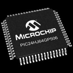
MCU 16-bit PIC24 PIC RISC 64KB Flash 3.3V 64-Pin QFN EP Tube, PIC24HJ64GP506A-E/MR, Microchip

PIC24HJ64GP506A is 16-bit Microcontrollers (up to 256 KB Flash and 16 KB SRAM) with Advanced Analog The PIC24H Family of devices is ideal for a wide vari- ety of 16-bit MCU embedded applications The PIC24HJXXXGPX06A/X08A /X10A device family includes devices with different pin counts (64 and 100 pins), different program memory sizes (64 Kbytes, 128 Kbytes and 256 Kbytes) and different RAM sizes (8 Kbytes and 16 Kbytes) This makes these families suitable for a wide variety of high-performance digital signal control applications. The devices are pin compatible with the dsPIC33F fam- ily of devices, and also share a very high degree of compatibility with the dsPIC30F family devices. This allows easy migration between device families as may be necessitated by the specific functionality, computa- tional resource and system cost requirements of the application The PIC24HJXXXGPX06A/X08A /X10A device family employs a powerful 16-bit architecture, ideal for applications that rely on high-speed, repetitive computations, as well as control The 17 x 17 multiplier, hardware support for division operations, multi-bit data shifter, a large array of 16-bit working registers and a wide variety of data addressing modes, together provide the PIC24HJXXXGPX06A/X08A/X10A Central Processing Unit (CPU) with extensive mathematical processing capability. Flexible and deterministic interrupt handling, coupled with a powerful array of peripherals, renders the PIC24HJXXXGPX06A/X08A /X10A devices suit- able for control applications. Further, Direct Memory Access (DMA) enables overhead-free transfer of data between several peripherals and a dedicated DMA RAM. Reliable, field programmable Flash program memory ensures scalability of applications that use PIC24HJXXXGPX06A/X08A/X10A devices

  • Core: 16-bit PIC24H CPU
  • Code-efficient (C and Assembly) architecture
  • Single-cycle mixed-sign MUL plus hardware divide
  • Clock Management
  • ±2% internal oscillator
  • Programmable PLLs and oscillator clock sources
  • Fail-Safe Clock Monitor (FSCM)
  • Independent Watchdog Timer (WDT)
  • Fast wake-up and start-up Power Management
  • Low-power management modes (Sleep, Idle, Doze)
  • Integrated Power-on Reset and Brown-out Reset
  • 1.35 mA/MHz dynamic current (typical)
  • 55µA IPD current (typical)
  • Advanced Analog Features
  • Two ADC modules: – Configurable as 10-bit, 1.1 Msps with four S&H or 12-bit, 500 ksps with one S&H – 18 analog inputs on 64-pin devices and up to 32 analog inputs on 100-pin devices
  • Flexible and independent ADC trigger sources Timers/Output Compare/Input Capture
  • Up to nine 16-bit timers/counters. Can pair up to make four 32-bit timers.
  • Eight Output Compare modules configurable as timers/counters
  • Eight Input Capture modules Communication Interfaces
  • Two UART modules (10 Mbps) – With support for LIN 2.0 protocols and IrDA ®
  • Two 4-wire SPI modules (15 Mbps)
  • Up to two I 2 C™ modules (up to 1 Mbaud) with SMBus support
  • Up to two Enhanced CAN (ECAN) modules (1 Mbaud) with 2.0B support
  • Data Converter Interface (DCI) module with I 2 S codec support Input/Output
  • Sink/Source up to 10 mA (pin specific) for stan- dard V OH /V OL , up to 16 mA (pin specific) for non- standard V OH 1
  • 5V-tolerant pins
  • Selectable open drain, pull-ups, and pull-downs
  • Up to 5 mA overvoltage clamp current
  • External interrupts on all I/O pins Qualification and Class B Support
  • AEC-Q100 REVG (Grade 1 -40°C to +125°C)
  • AEC-Q100 REVG (Grade 0 -40°C to +150°C)
  • Class B Safety Library, IEC 60730 Debugger Development Support
  • In-circuit and in-application programming
  • Two program and two complex data breakpoints
  • IEEE 1149.2-compatible (JTAG) boundary scan
  • Trace and run-time watch

Характеристики

Schedule_b

8542310000

Operating_supply_voltage

3.3 V

Operating_temperature

-40 to 125 °C

Pin_count

64

Product_dimensions

9 x 9 x 0.88 mm

Program_memory_size

64 KB

Ram_size

8 KB

Screening_level

Extended

On_chip_adc

18-chx12-bit

Special_features

CAN Controller

Specifications

https://4donline.ihs.com/images/VipMasterIC/IC/MCHP/MCHPS03933/MCHPS03933-1.pdf?hkey=52A5661711E402568146F3353EA87419

Supplier_package

QFN EP

Watchdog

1

Max_speed

40 MHz

Number_of_timers

9

Бренд

Instruction_set_architecture

RISC

Country_of_origin

Thailand

Data_bus_width

16 Bit

Device_core

PIC

Eccn

3A991.A.2

Htsn

8542310001

Тип интерфейса

CAN/I2C/SPI/UART

Number_of_programmable_i_os

53

Lead_finish

Matte Tin

Max_expanded_memory_size

12 MB

Max_operating_supply_voltage

3.6 V

Max_processing_temp

260 °C

Min_operating_supply_voltage

3 V

Mounting

Surface Mount

Msl_level

1

Артикул: PIC24HJ64GP506A-E/MR

Описание

PIC24HJ64GP506A is 16-bit Microcontrollers (up to 256 KB Flash and 16 KB SRAM) with Advanced Analog The PIC24H Family of devices is ideal for a wide vari- ety of 16-bit MCU embedded applications The PIC24HJXXXGPX06A/X08A /X10A device family includes devices with different pin counts (64 and 100 pins), different program memory sizes (64 Kbytes, 128 Kbytes and 256 Kbytes) and different RAM sizes (8 Kbytes and 16 Kbytes) This makes these families suitable for a wide variety of high-performance digital signal control applications. The devices are pin compatible with the dsPIC33F fam- ily of devices, and also share a very high degree of compatibility with the dsPIC30F family devices. This allows easy migration between device families as may be necessitated by the specific functionality, computa- tional resource and system cost requirements of the application The PIC24HJXXXGPX06A/X08A /X10A device family employs a powerful 16-bit architecture, ideal for applications that rely on high-speed, repetitive computations, as well as control The 17 x 17 multiplier, hardware support for division operations, multi-bit data shifter, a large array of 16-bit working registers and a wide variety of data addressing modes, together provide the PIC24HJXXXGPX06A/X08A/X10A Central Processing Unit (CPU) with extensive mathematical processing capability. Flexible and deterministic interrupt handling, coupled with a powerful array of peripherals, renders the PIC24HJXXXGPX06A/X08A /X10A devices suit- able for control applications. Further, Direct Memory Access (DMA) enables overhead-free transfer of data between several peripherals and a dedicated DMA RAM. Reliable, field programmable Flash program memory ensures scalability of applications that use PIC24HJXXXGPX06A/X08A/X10A devices

  • Core: 16-bit PIC24H CPU
  • Code-efficient (C and Assembly) architecture
  • Single-cycle mixed-sign MUL plus hardware divide
  • Clock Management
  • ±2% internal oscillator
  • Programmable PLLs and oscillator clock sources
  • Fail-Safe Clock Monitor (FSCM)
  • Independent Watchdog Timer (WDT)
  • Fast wake-up and start-up Power Management
  • Low-power management modes (Sleep, Idle, Doze)
  • Integrated Power-on Reset and Brown-out Reset
  • 1.35 mA/MHz dynamic current (typical)
  • 55µA IPD current (typical)
  • Advanced Analog Features
  • Two ADC modules: – Configurable as 10-bit, 1.1 Msps with four S&H or 12-bit, 500 ksps with one S&H – 18 analog inputs on 64-pin devices and up to 32 analog inputs on 100-pin devices
  • Flexible and independent ADC trigger sources Timers/Output Compare/Input Capture
  • Up to nine 16-bit timers/counters. Can pair up to make four 32-bit timers.
  • Eight Output Compare modules configurable as timers/counters
  • Eight Input Capture modules Communication Interfaces
  • Two UART modules (10 Mbps) – With support for LIN 2.0 protocols and IrDA ®
  • Two 4-wire SPI modules (15 Mbps)
  • Up to two I 2 C™ modules (up to 1 Mbaud) with SMBus support
  • Up to two Enhanced CAN (ECAN) modules (1 Mbaud) with 2.0B support
  • Data Converter Interface (DCI) module with I 2 S codec support Input/Output
  • Sink/Source up to 10 mA (pin specific) for stan- dard V OH /V OL , up to 16 mA (pin specific) for non- standard V OH 1
  • 5V-tolerant pins
  • Selectable open drain, pull-ups, and pull-downs
  • Up to 5 mA overvoltage clamp current
  • External interrupts on all I/O pins Qualification and Class B Support
  • AEC-Q100 REVG (Grade 1 -40°C to +125°C)
  • AEC-Q100 REVG (Grade 0 -40°C to +150°C)
  • Class B Safety Library, IEC 60730 Debugger Development Support
  • In-circuit and in-application programming
  • Two program and two complex data breakpoints
  • IEEE 1149.2-compatible (JTAG) boundary scan
  • Trace and run-time watch

Детали

Schedule_b

8542310000

Operating_supply_voltage

3.3 V

Operating_temperature

-40 to 125 °C

Pin_count

64

Product_dimensions

9 x 9 x 0.88 mm

Program_memory_size

64 KB

Ram_size

8 KB

Screening_level

Extended

On_chip_adc

18-chx12-bit

Special_features

CAN Controller

Specifications

https://4donline.ihs.com/images/VipMasterIC/IC/MCHP/MCHPS03933/MCHPS03933-1.pdf?hkey=52A5661711E402568146F3353EA87419

Supplier_package

QFN EP

Watchdog

1

Max_speed

40 MHz

Number_of_timers

9

Бренд

Instruction_set_architecture

RISC

Country_of_origin

Thailand

Data_bus_width

16 Bit

Device_core

PIC

Eccn

3A991.A.2

Htsn

8542310001

Тип интерфейса

CAN/I2C/SPI/UART

Number_of_programmable_i_os

53

Lead_finish

Matte Tin

Max_expanded_memory_size

12 MB

Max_operating_supply_voltage

3.6 V

Max_processing_temp

260 °C

Min_operating_supply_voltage

3 V

Mounting

Surface Mount

Msl_level

1