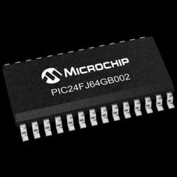
MCU 16-bit PIC24 PIC RISC 64KB Flash 2.5V/3.3V 28-Pin SOIC W, PIC24FJ64GB002-I/SO, Microchip

This family expands on the existing line of Microchip‘s 16-bit microcontrollers, combining an expanded peripheral feature set and enhanced computational performance with a new connectivity option: USB On-The-Go (OTG). The PIC24FJ64GB004 family provides a new platform for high-performance USB applications which may need more than an 8-bit platform, but do not require the power of a digital signal processor. Core Features 16-BIT ARCHITECTURE Central to all PIC24F devices is the 16-bit modified Harvard architecture, first introduced with Microchip’s dsPIC digital signal controllers. The PIC24F CPU core offers a wide range of enhancements, such as: 16-bit data and 24-bit address paths with the ability to move information between data and memory spaces Linear addressing of up to 12 Mbytes (program space) and 64 Kbytes (data) A 16-element working register array with built-in software stack support A 17 x 17 hardware multiplier with support for integer math Hardware support for 32 by 16-bit division An instruction set that supports multiple addressing modes and is optimized for high-level languages, such as ‘C’ Operational performance up to 16 MIPS POWER-SAVING TECHNOLOGY All of the devices in the PIC24FJ64GB004 family incorporate a range of features that can significantly reduce power consumption during operation. Key items include: On-the-Fly Clock Switching: The device clock can be changed under software control to the Timer1 source or the internal, Low-Power Internal RC Oscillator during operation, allowing the user to incorporate power-saving ideas into their software designs. Doze Mode Operation: When timing-sensitive applications, such as serial communications, require the uninterrupted operation of peripherals, the CPU clock speed can be selectively reduced, allowing incremental power savings without missing a beat. Instruction-Based Power-Saving Modes: There are three instruction-based power-saving modes: – Idle Mode – The core is shut down while leaving the peripherals active. – Sleep Mode – The core and peripherals that require the system clock are shut down, leaving the peripherals active that use their own clock or the clock from other devices. – Deep Sleep Mode – The core, peripherals (except RTCC and DSWDT), Flash and SRAM are shut down for optimal current savings to extend battery life for portable applications. OSCILLATOR OPTIONS AND FEATURES All of the devices in the PIC24FJ64GB004 family offer five different oscillator options, allowing users a range of choices in developing application hardware. These include: Two Crystal modes using crystals or ceramic resonators. Two External Clock modes offering the option of a divide-by-2 clock output. A Fast Internal RC Oscillator (FRC) with a nominal 8 MHz output, which can also be divided under software control to provide clock speeds as low as 31 kHz. A Phase Lock Loop (PLL) frequency multiplier available to the external oscillator modes and the FRC Oscillator, which allows clock speeds of up to 32 MHz. A separate Low-Power Internal RC Oscillator (LPRC) with a fixed 31 kHz output, which provides a low-power option for timing-insensitive applications. The internal oscillator block also provides a stable reference source for the Fail-Safe Clock Monitor. This option constantly monitors the main clock source against a reference signal provided by the internal oscillator and enables the controller to switch to the internal oscillator, allowing for continued low-speed operation or a safe application shutdown.

  • Universal Serial Bus Features:
  • USB v2.0 On- The- Go (OTG) Compliant
  • Dual Role Capable – Can act as either Host or Peripheral
  • Low- Speed (1.5 Mbps) and Full- Speed (12 Mbps) USB Operation in Host mode
  • Full Speed USB Operation in Device mode
  • High Precision PLL for USB
  • Supports up to 32 Endpoints (16 bidirectional):
    • USB module can use the internal RAM location from 0x800 to 0xFFFF as USB endpoint buffers
  • On Chip USB Transceiver with Interface for Off- Chip Transceiver
  • Supports Control, Interrupt, Isochronous and Bulk Transfers
  • On- Chip Pull- up and Pull- Down Resistors
  • Peripheral Features:
  • Enhanced Parallel Master Port/Parallel Slave Port (EPMP/PSP):
    • Direct access from CPU with an Extended Data Space (EDS) interface
    • 4, 8 and 16- bit wide data bus
    • Up to 23 programmable address lines
    • Up to 2 chip select lines
    • Up to 2 Acknowledgement lines (one per chip select)
    • Programmable address/data multiplexing
    • Programmable address and data Wait states
    • Programmable polarity on control signals
  • Peripheral Pin Select:
    • Up to 44 available pins (100- pin devices)
  • Three 3- Wire/4- Wire SPI modules (supports 4 Frame modes)
  • Three I2C modules Supporting Multi- Master/Slave modes and 7- Bit/10- Bit Addressing
  • Four UART modules:
    • Supports RS- 485, RS- 232, LIN/J2602 protocols and IrDA
  • Five 16- Bit Timers/Counters with Programmable Prescaler
  • Nine 16- Bit Capture Inputs, each with a Dedicated Time Base
  • Nine 16- Bit Compare/PWM Outputs, each with a Dedicated Time Base
  • Hardware Real- Time Clock and Calendar (RTCC)
  • Enhanced Programmable Cyclic Redundancy Check (CRC) Generator
  • Up to 5 External Interrupt Sources High- Performance CPU
  • Modified Harvard Architecture
  • Up to 16 MIPS Operation at 32 MHz
  • 8 MHz Internal Oscillator
  • 17- Bit x 17- Bit Single- Cycle Hardware Multiplier
  • 32- Bit by 16- Bit Hardware Divider
  • 16 x 16- Bit Working Register Array
  • C Compiler Optimized Instruction Set Architecture with Flexible Addressing modes
  • Linear Program Memory Addressing, up to 12 Mbytes
  • Data Memory Addressing, up to 16 Mbytes:
    • 2K SFR space
    • 30K linear data memory
    • 66K extended data memory
    • Remaining (from 16 Mbytes) memory (external) can be accessed using extended data Memory (EDS) and EPMP (EDS is divided into 32- Kbyte pages)
  • Two Address Generation Units for Separate Read and Write Addressing of Data Memory Power Management:
  • On- Chip Voltage Regulator of 1.8V
  • Switch between Clock Sources in Real Time
  • Idle, Sleep and Doze modes with Fast Wake- up and Two- Speed Start- up
  • Run Mode: 800 µA/MIPS, 3.3V Typical
  • Sleep mode Current Down to 20 µA, 3.3V Typical
  • Standby Current with 32 kHz Oscillator: 22 µA, 3.3V Typical
  • Analog Features:
  • 10- Bit, up to 24- Channel Analog- to- Digital (A/D) Converter at 500 ksps:
    • Operation is possible in Sleep mode
    • Band gap reference input feature

Характеристики

Schedule_b

8542310000

Operating_supply_voltage

2.5, 3.3 V

Operating_temperature

-40 to 85 °C

Pin_count

28

Product_dimensions

17.9 x 7.5 x 2.05 mm

Program_memory_size

64 KB

Ram_size

8 KB

Screening_level

Industrial

On_chip_adc

9-chx10-bit

Specifications

https://4donline.ihs.com/images/VipMasterIC/IC/MCHP/MCHP-S-A0006116192/MCHP-S-A0006116192-1.pdf?hkey=52A5661711E402568146F3353EA87419

Supplier_package

SOIC W

Watchdog

2

Max_speed

32 MHz

Number_of_timers

5

Бренд

Instruction_set_architecture

RISC

Country_of_origin

Thailand

Data_bus_width

16 Bit

Device_core

PIC

Eccn

3A991.A.2

Htsn

8542310001

Тип интерфейса

I2C/SPI/UART/USB

Number_of_programmable_i_os

19

Lead_finish

Matte Tin

Max_operating_supply_voltage

3.6 V

Max_processing_temp

260 °C

Min_operating_supply_voltage

2 V

Mounting

Surface Mount

Msl_level

1, 3

Артикул: PIC24FJ64GB002-I/SO

Описание

This family expands on the existing line of Microchip‘s 16-bit microcontrollers, combining an expanded peripheral feature set and enhanced computational performance with a new connectivity option: USB On-The-Go (OTG). The PIC24FJ64GB004 family provides a new platform for high-performance USB applications which may need more than an 8-bit platform, but do not require the power of a digital signal processor. Core Features 16-BIT ARCHITECTURE Central to all PIC24F devices is the 16-bit modified Harvard architecture, first introduced with Microchip’s dsPIC digital signal controllers. The PIC24F CPU core offers a wide range of enhancements, such as: 16-bit data and 24-bit address paths with the ability to move information between data and memory spaces Linear addressing of up to 12 Mbytes (program space) and 64 Kbytes (data) A 16-element working register array with built-in software stack support A 17 x 17 hardware multiplier with support for integer math Hardware support for 32 by 16-bit division An instruction set that supports multiple addressing modes and is optimized for high-level languages, such as ‘C’ Operational performance up to 16 MIPS POWER-SAVING TECHNOLOGY All of the devices in the PIC24FJ64GB004 family incorporate a range of features that can significantly reduce power consumption during operation. Key items include: On-the-Fly Clock Switching: The device clock can be changed under software control to the Timer1 source or the internal, Low-Power Internal RC Oscillator during operation, allowing the user to incorporate power-saving ideas into their software designs. Doze Mode Operation: When timing-sensitive applications, such as serial communications, require the uninterrupted operation of peripherals, the CPU clock speed can be selectively reduced, allowing incremental power savings without missing a beat. Instruction-Based Power-Saving Modes: There are three instruction-based power-saving modes: – Idle Mode – The core is shut down while leaving the peripherals active. – Sleep Mode – The core and peripherals that require the system clock are shut down, leaving the peripherals active that use their own clock or the clock from other devices. – Deep Sleep Mode – The core, peripherals (except RTCC and DSWDT), Flash and SRAM are shut down for optimal current savings to extend battery life for portable applications. OSCILLATOR OPTIONS AND FEATURES All of the devices in the PIC24FJ64GB004 family offer five different oscillator options, allowing users a range of choices in developing application hardware. These include: Two Crystal modes using crystals or ceramic resonators. Two External Clock modes offering the option of a divide-by-2 clock output. A Fast Internal RC Oscillator (FRC) with a nominal 8 MHz output, which can also be divided under software control to provide clock speeds as low as 31 kHz. A Phase Lock Loop (PLL) frequency multiplier available to the external oscillator modes and the FRC Oscillator, which allows clock speeds of up to 32 MHz. A separate Low-Power Internal RC Oscillator (LPRC) with a fixed 31 kHz output, which provides a low-power option for timing-insensitive applications. The internal oscillator block also provides a stable reference source for the Fail-Safe Clock Monitor. This option constantly monitors the main clock source against a reference signal provided by the internal oscillator and enables the controller to switch to the internal oscillator, allowing for continued low-speed operation or a safe application shutdown.

  • Universal Serial Bus Features:
  • USB v2.0 On- The- Go (OTG) Compliant
  • Dual Role Capable – Can act as either Host or Peripheral
  • Low- Speed (1.5 Mbps) and Full- Speed (12 Mbps) USB Operation in Host mode
  • Full Speed USB Operation in Device mode
  • High Precision PLL for USB
  • Supports up to 32 Endpoints (16 bidirectional):
    • USB module can use the internal RAM location from 0x800 to 0xFFFF as USB endpoint buffers
  • On Chip USB Transceiver with Interface for Off- Chip Transceiver
  • Supports Control, Interrupt, Isochronous and Bulk Transfers
  • On- Chip Pull- up and Pull- Down Resistors
  • Peripheral Features:
  • Enhanced Parallel Master Port/Parallel Slave Port (EPMP/PSP):
    • Direct access from CPU with an Extended Data Space (EDS) interface
    • 4, 8 and 16- bit wide data bus
    • Up to 23 programmable address lines
    • Up to 2 chip select lines
    • Up to 2 Acknowledgement lines (one per chip select)
    • Programmable address/data multiplexing
    • Programmable address and data Wait states
    • Programmable polarity on control signals
  • Peripheral Pin Select:
    • Up to 44 available pins (100- pin devices)
  • Three 3- Wire/4- Wire SPI modules (supports 4 Frame modes)
  • Three I2C modules Supporting Multi- Master/Slave modes and 7- Bit/10- Bit Addressing
  • Four UART modules:
    • Supports RS- 485, RS- 232, LIN/J2602 protocols and IrDA
  • Five 16- Bit Timers/Counters with Programmable Prescaler
  • Nine 16- Bit Capture Inputs, each with a Dedicated Time Base
  • Nine 16- Bit Compare/PWM Outputs, each with a Dedicated Time Base
  • Hardware Real- Time Clock and Calendar (RTCC)
  • Enhanced Programmable Cyclic Redundancy Check (CRC) Generator
  • Up to 5 External Interrupt Sources High- Performance CPU
  • Modified Harvard Architecture
  • Up to 16 MIPS Operation at 32 MHz
  • 8 MHz Internal Oscillator
  • 17- Bit x 17- Bit Single- Cycle Hardware Multiplier
  • 32- Bit by 16- Bit Hardware Divider
  • 16 x 16- Bit Working Register Array
  • C Compiler Optimized Instruction Set Architecture with Flexible Addressing modes
  • Linear Program Memory Addressing, up to 12 Mbytes
  • Data Memory Addressing, up to 16 Mbytes:
    • 2K SFR space
    • 30K linear data memory
    • 66K extended data memory
    • Remaining (from 16 Mbytes) memory (external) can be accessed using extended data Memory (EDS) and EPMP (EDS is divided into 32- Kbyte pages)
  • Two Address Generation Units for Separate Read and Write Addressing of Data Memory Power Management:
  • On- Chip Voltage Regulator of 1.8V
  • Switch between Clock Sources in Real Time
  • Idle, Sleep and Doze modes with Fast Wake- up and Two- Speed Start- up
  • Run Mode: 800 µA/MIPS, 3.3V Typical
  • Sleep mode Current Down to 20 µA, 3.3V Typical
  • Standby Current with 32 kHz Oscillator: 22 µA, 3.3V Typical
  • Analog Features:
  • 10- Bit, up to 24- Channel Analog- to- Digital (A/D) Converter at 500 ksps:
    • Operation is possible in Sleep mode
    • Band gap reference input feature

Детали

Schedule_b

8542310000

Operating_supply_voltage

2.5, 3.3 V

Operating_temperature

-40 to 85 °C

Pin_count

28

Product_dimensions

17.9 x 7.5 x 2.05 mm

Program_memory_size

64 KB

Ram_size

8 KB

Screening_level

Industrial

On_chip_adc

9-chx10-bit

Specifications

https://4donline.ihs.com/images/VipMasterIC/IC/MCHP/MCHP-S-A0006116192/MCHP-S-A0006116192-1.pdf?hkey=52A5661711E402568146F3353EA87419

Supplier_package

SOIC W

Watchdog

2

Max_speed

32 MHz

Number_of_timers

5

Бренд

Instruction_set_architecture

RISC

Country_of_origin

Thailand

Data_bus_width

16 Bit

Device_core

PIC

Eccn

3A991.A.2

Htsn

8542310001

Тип интерфейса

I2C/SPI/UART/USB

Number_of_programmable_i_os

19

Lead_finish

Matte Tin

Max_operating_supply_voltage

3.6 V

Max_processing_temp

260 °C

Min_operating_supply_voltage

2 V

Mounting

Surface Mount

Msl_level

1, 3