Описание
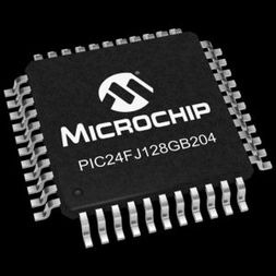
The PIC24FJ128GB204 family expands the capabilities of the PIC24F family by adding a complete selection of Cryptographic Engines, ISO 7816 support and I2S support to its existing features. This combination, along with its ultra low-power features, Direct Memory Access (DMA) for peripherals and USB On-The-Go, make this family the new standard for mixed-signal PIC microcontrollers in one economical and power-saving package. Core Features 16-BIT ARCHITECTURE Central to all PIC24F devices is the 16-bit modified Harvard architecture, first introduced with Microchip’s dsPIC Digital Signal Controllers (DSCs). The PIC24F CPU core offers a wide range of enhancements, such as: 16-bit data and 24-bit address paths with the ability to move information between data and memory spaces Linear addressing of up to 12 Mbytes (program space) and 32 Kbytes (data) A 16-element Working register array with built-in software stack support A 17 x 17 hardware multiplier with support for integer math Hardware support for 32 by 16-bit division An instruction set that supports multiple addressing modes and is optimized for high-level languages, such as ‘C’ Operational performance up to 16 MIPS XLP POWER-SAVING TECHNOLOGY The PIC24FJ128GB204 family of devices introduces a greatly expanded range of power-saving operating modes for the ultimate in power conservation. The new modes include: Retention Sleep with essential circuits being powered from a separate low-voltage regulator Deep Sleep without RTCC for the lowest possible power consumption under software control VBAT mode (with or without RTCC) to continue limited operation from a backup battery when VDD is removed Many of these new low-power modes also support the continuous operation of the low-power, on-chip Real-Time Clock/Calendar (RTCC), making it possible for an application to keep time while the device is otherwise asleep. Aside from these new features, PIC24FJ128GB204 family devices also include all of the legacy power-saving features of previous PIC24F microcontrollers, such as: On-the-Fly Clock Switching, allowing the selection of a lower power clock during run time Doze Mode Operation, for maintaining peripheral clock speed while slowing the CPU clock Instruction-Based Power-Saving Modes, for quick invocation of Idle and the many Sleep modes OSCILLATOR OPTIONS AND FEATURES All of the devices in the PIC24FJ128GB204 family offer five different oscillator options, allowing users a range of choices in developing application hardware. These include: Two Crystal modes Two External Clock modes A Phase Lock Loop (PLL) frequency multiplier, which allows clock speeds of up to 32 MHz A Fast Internal Oscillator (FRC) – Nominal 8 MHz output with multiple frequency divider options and automatic frequency self-calibration during run time A separate Low-Power Internal RC Oscillator (LPRC) – 31 kHz nominal for low-power, timing-insensitive applications. The internal oscillator block also provides a stable reference source for the Fail-Safe Clock Monitor (FSCM). This option constantly monitors the main clock source against a reference signal provided by the internal oscillator and enables the controller to switch to the internal oscillator, allowing for continued low-speed operation or a safe application shutdown. EASY MIGRATION Regardless of the memory size, all devices share the same rich set of peripherals, allowing for a smooth migration path as applications grow and evolve. This extends the ability of applications to grow from the relatively simple, to the powerful and complex, yet still selecting a Microchip device.
- Analog Features
- 10/12- Bit, 12- Channel Analog- to- Digital (A/D) Converter:
- Conversion rate of 500 ksps (10- bit), 200 ksps (12- bit)
- Conversion available during Sleep and Idle
- Three Rail- to- Rail, Enhanced Analog Comparators with Programmable Input/Output Configuration
- Three On- Chip Programmable Voltage References
- Charge Time Measurement Unit (CTMU):
- Used for capacitive touch sensing, up to 12 channels
- Time measurement down to 100 ps resolution
- Operation in Sleep mode
- Peripheral Features
- Up to Five External Interrupt Sources
- Peripheral Pin Select (PPS); Allows Independent I/O Mapping of many Peripherals
- Five 16- Bit Timers/Counters with Prescaler:
- Can be paired as 32- bit timers/counters
- Six- Channel DMA supports All Peripheral modules:
- Minimizes CPU overhead and increases data throughput
- Six Input Capture modules, each with a Dedicated 16- Bit Timer
- Six Output Compare/PWM modules, each with a Dedicated 16- Bit Timer
- Enhanced Parallel Master/Slave Port (EPMP/EPSP)
- Hardware Real- Time Clock/Calendar (RTCC):
- Runs in Sleep, Deep Sleep and VBAT modes
- Three 3- Wire/4- Wire SPI modules:
- Support four Frame modes
- Variable FIFO buffer
- I2S mode
- Variable width from 2- bit to 32- bit
- Two I2C™ modules Support Multi- Master/Slave mode and 7- Bit/10- Bit Addressing
- Four UART modules:
- Support RS- 485, RS- 232 and LIN/J2602
- On- chip hardware encoder/decoder for IrDA®
- Smart Card ISO 7816 support on UART1 and UART2 only:
- T = 0 protocol with automatic error handling
- T = 1 protocol
- Dedicated Guard Time Counter (GTC)
- Dedicated Waiting Time Counter (WTC)
- Auto- wake- up on Auto- Baud Detect (ABD)
- 4- level deep FIFO buffer
- Programmable 32- Bit Cyclic Redundancy Check (CRC) Generator
- Digital Signal Modulator provides On- Chip FSK and PSK Modulation for a Digital Signal Stream
- High- Current Sink/Source (18 mA/18 mA) on All I/O Pins
- Configurable Open- Drain Outputs on Digital I/O Pins
- 5.5V Tolerant Inputs on Most Pins
- High Performance CPU
- Modified Harvard Architecture
- Up to 16 MIPS Operation @ 32 MHz
- 8 MHz Internal Oscillator:
- 96 MHz PLL option
- Multiple clock divide options
- Run- time self- calibration capability for maintaining better than ±0.20% accuracy
- Fast start- up
- 17- Bit x 17- Bit Single- Cycle Hardware Fractional/Integer Multiplier
- 32- Bit by 16- Bit Hardware Divider
- 16 x 16- Bit Working Register Array
- C Compiler Optimized Instruction Set Architecture (ISA)
- Two Address Generation Units (AGUs) for Separate Read and Write Addressing of Data Memory
- Special Microcontroller Features
- Supply Voltage Range of 2.0V to 3.6V
- Two On- Chip Voltage Regulators (1.8V and 1.2V) for Regular and Extreme Low- Power Operation
- 20,000 Erase/Write Cycle Endurance Flash Program Memory, Typical
- Flash Data Retention: 20 Years Minimum
- Self- Programmable under Software Control
- Programmable Reference Clock Output
- In- Circuit Serial Programming™ (ICSP™) and In- Circuit Emulation (ICE) via 2 Pins
- JTAG Programming and Boundary Scan Support
- Fail- Safe Clock Monitor (FSCM) Operation:
- Detects clock failure and switches to on- chip, Low- Power RC Oscillator


