Описание
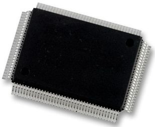
The H8S/2655 Group is a series of microcomputers (MCUs: microcomputer units), built around the H8S/2600 CPU, employing Renesas Technology proprietary architecture, and equipped with peripheral functions on-chip.The H8S/2600 CPU has an internal 32-bit architecture, is provided with sixteen 16-bit general registers and a concise, optimized instruction set designed for high-speed operation, and can address a 16-Mbyte linear address space. The instruction set is upward-compatible with H8/300 and H8/300H CPU instructions at the object-code level, facilitating migration from the H8/300,H8/300L, or H8/300H Series.On-chip peripheral functions required for system configuration include DMA controller (DMAC) and data transfer controller (DTC) bus masters, ROM and RAM, a16-bit timer-pulse unit (TPU),programmable pulse generator (PPG), 8-bit timer, watchdog timer (WDT), serial communication interface (SCI), A/D converter, D/A converter, and I/O ports.The on-chip ROM is either PROM (ZTAT) or mask ROM, with a capacity of 128 or 64 kbytes. ROM is connected to the CPU via a 16-bit data bus, enabling both byte and word data to be accessed in one state. Instruction fetching has been speeded up, and processing speed increased.Seven operating modes, modes 1 to 7, are provided, and there is a choice of address space and single-chip mode or external expansion mode.
- General-register machine
- Sixteen 16-bit general registers (also usable as sixteen 8-bit registers or eight 32-bit registers)
- High-speed operation suitable for real time control
- Maximum clock rate: 20 MHz
- High-speed arithmetic operations
- 8/16/32-bit register-register add/subtract: 50 ns
- 16 × 16-bit register-register multiply: 200 ns
- 16 × 16 + 42-bit multiply and accumulate: 200 ns
- 32 ÷ 16-bit register-register divide: 1000 ns
- Instruction set suitable for high-speed operation
- Sixty-nine basic instructions
- 8/16/32-bit move/arithmetic and logic instructions
- Unsigned/signed multiply and divide instructions
- Multiply-and accumulate instruction
- Powerful bit-manipulation instructions
- Two CPU operating modes
- Normal mode: 64-kbyte address space
- Advanced mode: 16-Mbyte address space