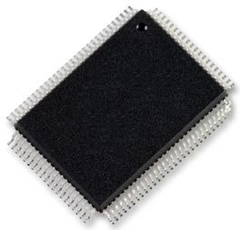
MCU 16-bit/32-bit H8 CISC 60KB ROM 3.3V/5V 100-Pin PQFP, HD6473837FV, Renesas Electronics

The H8/300L Series is a series of single-chip microcomputers (MCU: microcomputer unit), built around the high-speed H8/300L CPU and equipped with peripheral system functions on-chip.Within the H8/300L Series, the H8/3834 Series features an on-chip liquid crystal display (LCD) controller/driver. Other on-chip peripheral functions include five timers, a 14-bit pulse width modulator (PWM), three serial communication interface channels, and an analog-to-digital (A/D) converter. Together these functions make the H8/3834 Series ideally suited for embedded control of systems requiring an LCD display.

  • CPU : High-speed H8/300L CPU
    • General-register architecture
    • General registers: Sixteen 8-bit registers (can be used as eight 16-bit registers)
    • Operating speed
    • Max. operating speed: 5 MHz
    • Add/subtract: 0.4 µs (operating at 5 MHz)
    • Multiply/divide: 2.8 µs (operating at 5 MHz)
    • Can run on 32.768 kHz subclock
    • Instruction set compatible with H8/300 CPU
    • Instruction length of 2 bytes or 4 bytes
    • Basic arithmetic operations between registers
    • MOV instruction for data transfer between memory and registers
    • Typical instructions
    • Multiply (8 bits × 8 bits)
    • Divide (16 bits ÷ 8 bits)
    • Bit accumulator
    • Register-indirect designation of bit position
  • Interrupts 33 interrupt sources
    • 13 external interrupt pins: IRQ4 to IRQ0, WKP7 to WKP0
    • 20 internal interrupt sources
  • Clock pulse generators Two on-chip clock pulse generators
    • System clock pulse generator: 1 to 10 MHz
    • Subclock pulse generator: 32.768 kH
  • Power-down modes Six power-down modes
    • Sleep mode
    • Standby mode
    • Watch mode
    • Subsleep mode
    • Subactive mode
    • Active (medium-speed) mode
  • Memory
    • Large on-chip memory
    • 32-kbyte ROM, 1-kbyte RAM
  • I/O ports
    • 84 I/O port pins
    • I/O pins: 71
    • Input pins: 13
  • Timers
    • Five on-chip timers
    • Timer A: 8-bit timer
    • Timer B: 8-bit timer
    • Count-up timer with selection of seven internal clock signals or event input from external pin
    • Auto-reloading
    • Timer C: 8-bit timer
    • Count-up/count-down timer with selection of seven internal clock signals or event input from external pin
    • Auto-reloading
    • Timer F: 16-bit timer
    • Can be used as two independent 8-bit timers.
    • Count-up timer with selection of four internal clock signals or event input from external pin
    • Compare-match function with toggle output
    • Timer G: 8-bit timer
    • Count-up timer with selection of four internal clock signals
    • Input capture function with built-in noise canceller circuit
  • Serial communication interface
    • Three channels on chip
    • SCI1: synchronous serial interface Choice of 8-bit or 16-bit data transfer
    • SCI2: 8-bit synchronous serial interface
    • Automatic transfer of 32-byte data segments
    • SCI3: 8-bit synchronous or asynchronous serial interface
    • Built-in function for multiprocessor communication
  • 14-bit PWM
    • Pulse-division PWM output for reduced ripple
    • Can be used as a 14-bit D/A converter by connecting to an external low-pass filter.
  • A/D converter
    • Successive approximations using a resistance ladder resolution: 8 bits
    • 12-channel analog input port
    • Conversion time: 31/f or 62/f per channel
  • LCD controller/driver
    • Up to 40 segment pins and 4 common pins
    • Choice of four duty cycles (static, 1/2, 1/3, 1/4)
    • Segments can be expanded externally
    • Segment pins can be switched to general-purpose ports in groups of four

Характеристики

Schedule_b

8542320040

Operating_supply_voltage

3.3, 5 V

Operating_temperature

-20 to 75 °C

Pin_count

100

Product_dimensions

20 x 14 x 2.7 mm

Program_memory_size

60 Kb

Ram_size

2 KB

On_chip_adc

12-chx8-bit

Specifications

https://4donline.ihs.com/images/VipMasterIC/IC/RNCC/RNCCS12907/RNCCS12907-1.pdf?hkey=52A5661711E402568146F3353EA87419

Supplier_package

PQFP

Max_speed

10 MHz

Number_of_timers

5

Бренд

Instruction_set_architecture

CISC

Country_of_origin

United States

Data_bus_width

16, 32 Bit

Eccn

EAR99

Htsn

8542320041

Тип интерфейса

SCI

Number_of_programmable_i_os

71

Lead_finish

Tin/Bismuth, Tin/Copper

Max_expanded_memory_size

64 KB

Max_operating_supply_voltage

5.5 V

Max_processing_temp

260 °C

Min_operating_supply_voltage

2.5 V

Mounting

Surface Mount

Msl_level

3

SKU: HD6473837FV

Description

The H8/300L Series is a series of single-chip microcomputers (MCU: microcomputer unit), built around the high-speed H8/300L CPU and equipped with peripheral system functions on-chip.Within the H8/300L Series, the H8/3834 Series features an on-chip liquid crystal display (LCD) controller/driver. Other on-chip peripheral functions include five timers, a 14-bit pulse width modulator (PWM), three serial communication interface channels, and an analog-to-digital (A/D) converter. Together these functions make the H8/3834 Series ideally suited for embedded control of systems requiring an LCD display.

  • CPU : High-speed H8/300L CPU
    • General-register architecture
    • General registers: Sixteen 8-bit registers (can be used as eight 16-bit registers)
    • Operating speed
    • Max. operating speed: 5 MHz
    • Add/subtract: 0.4 µs (operating at 5 MHz)
    • Multiply/divide: 2.8 µs (operating at 5 MHz)
    • Can run on 32.768 kHz subclock
    • Instruction set compatible with H8/300 CPU
    • Instruction length of 2 bytes or 4 bytes
    • Basic arithmetic operations between registers
    • MOV instruction for data transfer between memory and registers
    • Typical instructions
    • Multiply (8 bits × 8 bits)
    • Divide (16 bits ÷ 8 bits)
    • Bit accumulator
    • Register-indirect designation of bit position
  • Interrupts 33 interrupt sources
    • 13 external interrupt pins: IRQ4 to IRQ0, WKP7 to WKP0
    • 20 internal interrupt sources
  • Clock pulse generators Two on-chip clock pulse generators
    • System clock pulse generator: 1 to 10 MHz
    • Subclock pulse generator: 32.768 kH
  • Power-down modes Six power-down modes
    • Sleep mode
    • Standby mode
    • Watch mode
    • Subsleep mode
    • Subactive mode
    • Active (medium-speed) mode
  • Memory
    • Large on-chip memory
    • 32-kbyte ROM, 1-kbyte RAM
  • I/O ports
    • 84 I/O port pins
    • I/O pins: 71
    • Input pins: 13
  • Timers
    • Five on-chip timers
    • Timer A: 8-bit timer
    • Timer B: 8-bit timer
    • Count-up timer with selection of seven internal clock signals or event input from external pin
    • Auto-reloading
    • Timer C: 8-bit timer
    • Count-up/count-down timer with selection of seven internal clock signals or event input from external pin
    • Auto-reloading
    • Timer F: 16-bit timer
    • Can be used as two independent 8-bit timers.
    • Count-up timer with selection of four internal clock signals or event input from external pin
    • Compare-match function with toggle output
    • Timer G: 8-bit timer
    • Count-up timer with selection of four internal clock signals
    • Input capture function with built-in noise canceller circuit
  • Serial communication interface
    • Three channels on chip
    • SCI1: synchronous serial interface Choice of 8-bit or 16-bit data transfer
    • SCI2: 8-bit synchronous serial interface
    • Automatic transfer of 32-byte data segments
    • SCI3: 8-bit synchronous or asynchronous serial interface
    • Built-in function for multiprocessor communication
  • 14-bit PWM
    • Pulse-division PWM output for reduced ripple
    • Can be used as a 14-bit D/A converter by connecting to an external low-pass filter.
  • A/D converter
    • Successive approximations using a resistance ladder resolution: 8 bits
    • 12-channel analog input port
    • Conversion time: 31/f or 62/f per channel
  • LCD controller/driver
    • Up to 40 segment pins and 4 common pins
    • Choice of four duty cycles (static, 1/2, 1/3, 1/4)
    • Segments can be expanded externally
    • Segment pins can be switched to general-purpose ports in groups of four

Additional information

Schedule_b

8542320040

Operating_supply_voltage

3.3, 5 V

Operating_temperature

-20 to 75 °C

Pin_count

100

Product_dimensions

20 x 14 x 2.7 mm

Program_memory_size

60 Kb

Ram_size

2 KB

On_chip_adc

12-chx8-bit

Specifications

https://4donline.ihs.com/images/VipMasterIC/IC/RNCC/RNCCS12907/RNCCS12907-1.pdf?hkey=52A5661711E402568146F3353EA87419

Supplier_package

PQFP

Max_speed

10 MHz

Number_of_timers

5

Бренд

Instruction_set_architecture

CISC

Country_of_origin

United States

Data_bus_width

16, 32 Bit

Eccn

EAR99

Htsn

8542320041

Тип интерфейса

SCI

Number_of_programmable_i_os

71

Lead_finish

Tin/Bismuth, Tin/Copper

Max_expanded_memory_size

64 KB

Max_operating_supply_voltage

5.5 V

Max_processing_temp

260 °C

Min_operating_supply_voltage

2.5 V

Mounting

Surface Mount

Msl_level

3