Описание
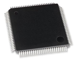
This LSI is a single-chip microcomputer made up of the H8S/2000 CPU with an internal 32-bit architecture as its core, and the peripheral functions required to configure a system. This LSI is equipped with ROM, RAM, a bus controller, data transfer controller (DTC), a 16-bit timer pulse unit (TPU), a watchdog timer (WDT), a serial communication interface (SCI), a D/A converter, an A/D converter, and I/O ports as on-chip supporting modules. This LSI is suitable for use as an embedded processor for high-level control systems. Its on-chip ROM are flash memory and mask ROM that provides flexibility as it can be reprogrammed in no time to cope with all situations from the early stages of mass production to full-scale mass production. This is particularly applicable to application devices with specifications that will most probably change.
- Operating frequency (MHz)/Supply voltage (V)
- 20MHz/2.7 to 3.6V (Mask, ROMless only)
- 25MHz/3.0 to 3.6V
- Minimum instruction execution time: 40ns/50ns
- On-chip memory 512kB/16kB