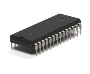
MCU 8-bit PIC18 PIC RISC 32KB Flash 2.5V/3.3V/5V 28-Pin SPDIP Tube, PIC18LF2550-I/SP, Microchip

PIC18LF2550 devices offers the advantages of all PIC18 microcontrollers – namely, high computational performance at an economical price – with the addition of high-endurance, Enhanced Flash program memory. In addition to these features, the PIC18F2455/2550/4455/4550 family introduces design enhancements that make these microcontrollers a logical choice for many high-performance, power sensitive applications. All of the devices in the PIC18F2455/2550/4455/4550 family incorporate a range of features that can significantly reduce power consumption during operation. Alternate Run Modes: By clocking the controller from the Timer1 source or the internal oscillator block, power consumption during code execution can be reduced by as much as 90%. Multiple Idle Modes: The controller can also run with its CPU core disabled but the peripherals still active. In these states, power consumption can be reduced even further, to as little as 4%, of normal operation requirements. On-the-Fly Mode Switching: The power-managed modes are invoked by user code during operation, allowing the user to incorporate power-saving ideas into their application’s software design. Low Consumption in Key Modules: The power requirements for both Timer1 and the Watchdog Timer are minimized. Devices in the PIC18F2455/2550/4455/4550 family incorporate a fully featured Universal Serial Bus communications module that is compliant with the USB Specification Revision 2.0. The module supports both low-speed and full-speed communication for all supported data transfer types. It also incorporates its own on-chip transceiver and 3.3V regulator and supports the use of external transceivers and voltage regulators. All of the devices in the PIC18F2455/2550/4455/4550 family offer twelve different oscillator options, allowing users a wide range of choices in developing application hardware. These include: Four Crystal modes using crystals or ceramic resonators. Four External Clock modes, offering the option of using two pins (oscillator input and a divide-by-4 clock output) or one pin (oscillator input, with the second pin reassigned as general I/O). An internal oscillator block which provides an 8 MHz clock (±2% accuracy) and an INTRC source (approximately 31 kHz, stable over temperature and VDD), as well as a range of 6 user-selectable clock frequencies, between 125 kHz to 4 MHz, for a total of 8 clock frequencies. This option frees an oscillator pin for use as an additional general purpose I/O. A Phase Lock Loop (PLL) frequency multiplier, available to both the High-Speed Crystal and External Oscillator modes, which allows a wide range of clock speeds from 4 MHz to 48 MHz. Asynchronous dual clock operation, allowing the USB module to run from a high-frequency oscillator while the rest of the microcontroller is clocked from an internal low-power oscillator Besides its availability as a clock source, the internal oscillator block provides a stable reference source that gives the family additional features for robust operation Fail-Safe Clock Monitor: This option constantly monitors the main clock source against a reference signal provided by the internal oscillator. If a clock failure occurs, the controller is switched to the internal oscillator block, allowing for continued low-speed operation or a safe application shutdown Two-Speed Start-up: This option allows the internal oscillator to serve as the clock source from Power-on Reset, or wake-up from Sleep mode, until the primary clock source is available

  • Universal Serial Bus Features:
  • USB V2.0 Compliant
  • Low Speed (1.5 Mb/s) and Full Speed (12 Mb/s)
  • Supports Control, Interrupt, Isochronous and Bulk Transfers
  • Supports up to 32 Endpoints (16 bidirectional)
  • 1 Kbyte Dual Access RAM for USB
  • On-Chip USB Transceiver with On-Chip Voltage Regulator
  • Interface for Off-Chip USB Transceiver
  • Streaming Parallel Port (SPP) for USB streaming transfers (40/44-pin devices only) Power-Managed Modes:
  • Run: CPU on, Peripherals on
  • Idle: CPU off, Peripherals on
  • Sleep: CPU off, Peripherals off
  • Idle mode Currents Down to 5.8 µA Typical
  • Sleep mode Currents Down to 0.1 µA Typical
  • Timer1 Oscillator: 1.1 µA Typical, 32 kHz, 2V
  • Watchdog Timer: 2.1 µA Typical
  • Two-Speed Oscillator Start-up Flexible Oscillator Structure:
  • Four Crystal modes, including High-Precision PLL for USB
  • Two External Clock modes, Up to 48 MHz
  • Internal Oscillator Block:
    • 8 user-selectable frequencies, from 31 kHz to 8 MHz
    • User-tunable to compensate for frequency drift
  • Secondary Oscillator using Timer1 @ 32 kHz
  • Dual Oscillator Options allow Microcontroller and USB module to Run at Different Clock Speeds
  • Fail-Safe Clock Monitor:
    • Allows for safe shutdown if any clock stops
  • Peripheral Highlights:
  • High-Current Sink/Source: 25 mA/25 mA
  • Three External Interrupts
  • Four Timer modules (Timer0 to Timer3)
  • Up to 2 Capture/Compare/PWM (CCP) modules:
    • Capture is 16-bit, max. resolution 5.2 ns (TCY/16)
    • Compare is 16-bit, max. resolution 83.3 ns (TCY)
    • PWM output: PWM resolution is 1 to 10-bit
  • Enhanced Capture/Compare/PWM (ECCP) module:
    • Multiple output modes
    • Selectable polarity
    • Programmable dead time
    • Auto-shutdown and auto-restart
  • Enhanced USART module:
    • LIN bus support
  • Master Synchronous Serial Port (MSSP) module Supporting 3-Wire SPI (all 4 modes) and I2C™ Master and Slave modes
  • 10-Bit, Up to 13-Channel Analog-to-Digital Converter (A/D) module with Programmable Acquisition Time
  • Dual Analog Comparators with Input Multiplexing Special Microcontroller Features:
  • C Compiler Optimized Architecture with Optional Extended Instruction Set
  • 100,000 Erase/Write Cycle Enhanced Flash Program Memory Typical
  • 1,000,000 Erase/Write Cycle Data EEPROM Memory Typical
  • Flash/Data EEPROM Retention: > 40 Years
  • Self-Programmable under Software Control
  • Priority Levels for Interrupts
  • 8 x 8 Single-Cycle Hardware Multiplier
  • Extended Watchdog Timer (WDT):
    • Programmable period from 41 ms to 131s
  • Programmable Code Protection
  • Single-Supply 5V In-Circuit Serial Programming™ (ICSP™) via Two Pins
  • In-Circuit Debug (ICD) via Two Pins
  • Optional Dedic

Характеристики

Analog_comparators

2

Operating_temperature

-40 to 85 °C

Max_power_dissipation

1000 mW

Min_operating_supply_voltage

2 V

Max_operating_supply_voltage

5.5 V

Watchdog

1

Supplier_package

SPDIP

Specifications

https://4donline.ihs.com/images/VipMasterIC/IC/MCHP/MCHPS03011/MCHPS03011-1.pdf?hkey=52A5661711E402568146F3353EA87419

Screening_level

Industrial

Schedule_b

8542310000

Ram_size

2 KB

Program_memory_type

Flash

Program_memory_size

32 Kb

Product_dimensions

34.67 x 7.24 x 3.3 mm

Pin_count

28

Operating_supply_voltage

2.5, 3.3, 5 V

Бренд

On_chip_adc

10-chx10-bit

Number_of_timers

4

Number_of_programmable_i_os

24

Mounting

Through Hole

Maximum_speed

48 MHz

Max_processing_temp

260

Lead_finish

Matte Tin

Тип интерфейса

I2C/SPI/USART/USB

Instruction_set_architecture

RISC

Htsn

8542310001

Eccn

3A991.A.2

Device_core

PIC

Data_bus_width

8 Bit

Country_of_origin

China

Max_expanded_memory_size

2 MB

SKU: PIC18LF2550-I/SP

Description

PIC18LF2550 devices offers the advantages of all PIC18 microcontrollers – namely, high computational performance at an economical price – with the addition of high-endurance, Enhanced Flash program memory. In addition to these features, the PIC18F2455/2550/4455/4550 family introduces design enhancements that make these microcontrollers a logical choice for many high-performance, power sensitive applications. All of the devices in the PIC18F2455/2550/4455/4550 family incorporate a range of features that can significantly reduce power consumption during operation. Alternate Run Modes: By clocking the controller from the Timer1 source or the internal oscillator block, power consumption during code execution can be reduced by as much as 90%. Multiple Idle Modes: The controller can also run with its CPU core disabled but the peripherals still active. In these states, power consumption can be reduced even further, to as little as 4%, of normal operation requirements. On-the-Fly Mode Switching: The power-managed modes are invoked by user code during operation, allowing the user to incorporate power-saving ideas into their application’s software design. Low Consumption in Key Modules: The power requirements for both Timer1 and the Watchdog Timer are minimized. Devices in the PIC18F2455/2550/4455/4550 family incorporate a fully featured Universal Serial Bus communications module that is compliant with the USB Specification Revision 2.0. The module supports both low-speed and full-speed communication for all supported data transfer types. It also incorporates its own on-chip transceiver and 3.3V regulator and supports the use of external transceivers and voltage regulators. All of the devices in the PIC18F2455/2550/4455/4550 family offer twelve different oscillator options, allowing users a wide range of choices in developing application hardware. These include: Four Crystal modes using crystals or ceramic resonators. Four External Clock modes, offering the option of using two pins (oscillator input and a divide-by-4 clock output) or one pin (oscillator input, with the second pin reassigned as general I/O). An internal oscillator block which provides an 8 MHz clock (±2% accuracy) and an INTRC source (approximately 31 kHz, stable over temperature and VDD), as well as a range of 6 user-selectable clock frequencies, between 125 kHz to 4 MHz, for a total of 8 clock frequencies. This option frees an oscillator pin for use as an additional general purpose I/O. A Phase Lock Loop (PLL) frequency multiplier, available to both the High-Speed Crystal and External Oscillator modes, which allows a wide range of clock speeds from 4 MHz to 48 MHz. Asynchronous dual clock operation, allowing the USB module to run from a high-frequency oscillator while the rest of the microcontroller is clocked from an internal low-power oscillator Besides its availability as a clock source, the internal oscillator block provides a stable reference source that gives the family additional features for robust operation Fail-Safe Clock Monitor: This option constantly monitors the main clock source against a reference signal provided by the internal oscillator. If a clock failure occurs, the controller is switched to the internal oscillator block, allowing for continued low-speed operation or a safe application shutdown Two-Speed Start-up: This option allows the internal oscillator to serve as the clock source from Power-on Reset, or wake-up from Sleep mode, until the primary clock source is available

  • Universal Serial Bus Features:
  • USB V2.0 Compliant
  • Low Speed (1.5 Mb/s) and Full Speed (12 Mb/s)
  • Supports Control, Interrupt, Isochronous and Bulk Transfers
  • Supports up to 32 Endpoints (16 bidirectional)
  • 1 Kbyte Dual Access RAM for USB
  • On-Chip USB Transceiver with On-Chip Voltage Regulator
  • Interface for Off-Chip USB Transceiver
  • Streaming Parallel Port (SPP) for USB streaming transfers (40/44-pin devices only) Power-Managed Modes:
  • Run: CPU on, Peripherals on
  • Idle: CPU off, Peripherals on
  • Sleep: CPU off, Peripherals off
  • Idle mode Currents Down to 5.8 µA Typical
  • Sleep mode Currents Down to 0.1 µA Typical
  • Timer1 Oscillator: 1.1 µA Typical, 32 kHz, 2V
  • Watchdog Timer: 2.1 µA Typical
  • Two-Speed Oscillator Start-up Flexible Oscillator Structure:
  • Four Crystal modes, including High-Precision PLL for USB
  • Two External Clock modes, Up to 48 MHz
  • Internal Oscillator Block:
    • 8 user-selectable frequencies, from 31 kHz to 8 MHz
    • User-tunable to compensate for frequency drift
  • Secondary Oscillator using Timer1 @ 32 kHz
  • Dual Oscillator Options allow Microcontroller and USB module to Run at Different Clock Speeds
  • Fail-Safe Clock Monitor:
    • Allows for safe shutdown if any clock stops
  • Peripheral Highlights:
  • High-Current Sink/Source: 25 mA/25 mA
  • Three External Interrupts
  • Four Timer modules (Timer0 to Timer3)
  • Up to 2 Capture/Compare/PWM (CCP) modules:
    • Capture is 16-bit, max. resolution 5.2 ns (TCY/16)
    • Compare is 16-bit, max. resolution 83.3 ns (TCY)
    • PWM output: PWM resolution is 1 to 10-bit
  • Enhanced Capture/Compare/PWM (ECCP) module:
    • Multiple output modes
    • Selectable polarity
    • Programmable dead time
    • Auto-shutdown and auto-restart
  • Enhanced USART module:
    • LIN bus support
  • Master Synchronous Serial Port (MSSP) module Supporting 3-Wire SPI (all 4 modes) and I2C™ Master and Slave modes
  • 10-Bit, Up to 13-Channel Analog-to-Digital Converter (A/D) module with Programmable Acquisition Time
  • Dual Analog Comparators with Input Multiplexing Special Microcontroller Features:
  • C Compiler Optimized Architecture with Optional Extended Instruction Set
  • 100,000 Erase/Write Cycle Enhanced Flash Program Memory Typical
  • 1,000,000 Erase/Write Cycle Data EEPROM Memory Typical
  • Flash/Data EEPROM Retention: > 40 Years
  • Self-Programmable under Software Control
  • Priority Levels for Interrupts
  • 8 x 8 Single-Cycle Hardware Multiplier
  • Extended Watchdog Timer (WDT):
    • Programmable period from 41 ms to 131s
  • Programmable Code Protection
  • Single-Supply 5V In-Circuit Serial Programming™ (ICSP™) via Two Pins
  • In-Circuit Debug (ICD) via Two Pins
  • Optional Dedic

Additional information

Analog_comparators

2

Operating_temperature

-40 to 85 °C

Max_power_dissipation

1000 mW

Min_operating_supply_voltage

2 V

Max_operating_supply_voltage

5.5 V

Watchdog

1

Supplier_package

SPDIP

Specifications

https://4donline.ihs.com/images/VipMasterIC/IC/MCHP/MCHPS03011/MCHPS03011-1.pdf?hkey=52A5661711E402568146F3353EA87419

Screening_level

Industrial

Schedule_b

8542310000

Ram_size

2 KB

Program_memory_type

Flash

Program_memory_size

32 Kb

Product_dimensions

34.67 x 7.24 x 3.3 mm

Pin_count

28

Operating_supply_voltage

2.5, 3.3, 5 V

Бренд

On_chip_adc

10-chx10-bit

Number_of_timers

4

Number_of_programmable_i_os

24

Mounting

Through Hole

Maximum_speed

48 MHz

Max_processing_temp

260

Lead_finish

Matte Tin

Тип интерфейса

I2C/SPI/USART/USB

Instruction_set_architecture

RISC

Htsn

8542310001

Eccn

3A991.A.2

Device_core

PIC

Data_bus_width

8 Bit

Country_of_origin

China

Max_expanded_memory_size

2 MB