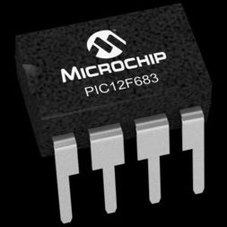
MCU 8-bit PIC12 PIC RISC 3.5KB Flash 5V 8-Pin SOIC N Tube, PIC12F683-I/SN, Microchip

Program Memory Organization The PIC12F683 has a 13-bit program counter capable of addressing an 8k x 14 program memory space. Only the first 2k x 14 (0000h-07FFh) for the PIC12F683 is physically implemented. Accessing a location above these boundaries will cause a wraparound within the first 2K x 14 space. The Reset vector is at 0000h and the interrupt vector is at 0004h. Data Memory Organization The data memory is partitioned into two banks, which contain the General Purpose Registers (GPR) and the Special Function Registers (SFR). The Special Function Registers are located in the first 32 locations of each bank. Register locations 20h-7Fh in Bank 0 and A0h-BFh in Bank 1 are General Purpose Registers, implemented as static RAM. Register locations F0h-FFh in Bank 1 point to addresses 70h-7Fh in Bank 0. All other RAM is unimplemented and returns ‘0’ when read. RP0 of the STATUS register is the bank select bit.

  • High-Performance RISC CPU:
  • Only 35 instructions to learn:
    • All single-cycle instructions except branches
  • Operating speed:
    • DC – 20 MHz oscillator/clock input
    • DC – 200 ns instruction cycle
  • Interrupt capability
  • 8-level deep hardware stack
  • Direct, Indirect and Relative Addressing modes
  • Special Microcontroller Features:
  • Precision Internal Oscillator:
    • Factory calibrated to ±1%, typical
    • Software selectable frequency range of 8 MHz to 125 kHz
    • Software tunable
    • Two-Speed Start-up mode
    • Crystal fail detect for critical applications
    • Clock mode switching during operation for power savings
  • Power-Saving Sleep mode
  • Wide operating voltage range (2.0V-5.5V)
  • Industrial and Extended temperature range
  • Power-on Reset (POR)
  • Power-up Timer (PWRT) and Oscillator Start-up Timer (OST)
  • Brown-out Reset (BOR) with software control option
  • Enhanced Low-Current Watchdog Timer (WDT) with on-chip oscillator (software selectable nominal 268 seconds with full prescaler) with software enable
  • Multiplexed Master Clear with pull-up/input pin
  • Programmable code protection
  • High Endurance Flash/EEPROM cell:
    • 100,000 write Flash endurance
    • 1,000,000 write EEPROM endurance
    • Flash/Data EEPROM Retention: > 40 years
  • Low-Power Features:
  • Standby Current:
    • 50 nA @ 2.0V, typical
  • Operating Current:
    • 11 µA @ 32 kHz, 2.0V, typical
    • 220 µA @ 4 MHz, 2.0V, typical
  • Watchdog Timer Current:
    • 1 µA @ 2.0V, typical
  • Peripheral Features:
  • 6 I/O pins with individual direction control:
    • High current source/sink for direct LED drive
    • Interrupt-on-pin change
    • Individually programmable weak pull-ups
    • Ultra Low-Power Wake-up on GP0
  • Analog Comparator module with:
    • One analog comparator
    • Programmable on-chip voltage reference (CVREF) module (% of VDD)
    • Comparator inputs and output externally accessible
  • A/D Converter:
    • 10-bit resolution and 4 channels
  • Timer0: 8-bit timer/counter with 8-bit programmable prescaler
  • Enhanced Timer1:
    • 16-bit timer/counter with prescaler
    • External Timer1 Gate (count enable)
    • Option to use OSC1 and OSC2 in LP mode as Timer1 oscillator if INTOSC mode selected
  • Timer2: 8-bit timer/counter with 8-bit period register, prescaler and postscaler
  • Capture, Compare, PWM module:
    • 16-bit Capture, max resolution 12.5 ns
    • Compare, max resolution 200 ns
    • 10-bit PWM, max frequency 20 kHz
  • In-Circuit Serial Programming™ (ICSP™) via two pins
Характеристики

Analog_comparators

1

Operating_supply_voltage

5 V

Max_power_dissipation

800 mW

Min_operating_supply_voltage

4.5 V

Max_operating_supply_voltage

5.5 V

Watchdog

1

Supplier_package

SOIC N

Specifications

https://4donline.ihs.com/images/VipMasterIC/IC/MCHP/MCHPS02365/MCHPS02365-1.pdf?hkey=52A5661711E402568146F3353EA87419

Screening_level

Industrial

Schedule_b

8542310000

Ram_size

128 byte

Program_memory_type

Flash

Program_memory_size

3.5 KB

Product_dimensions

4.9 x 3.9 x 1.25 mm

Pin_count

8

Operating_temperature

-40 to 85 °C

On_chip_adc

4-chx10-bit

Бренд

Number_of_timers

3

Number_of_programmable_i_os

6

Msl_level

1

Mounting

Surface Mount

Maximum_speed

20 MHz

Max_processing_temp

260

Lead_finish

Matte Tin

Instruction_set_architecture

RISC

Htsn

8542310001

Eccn

EAR99

Device_core

PIC

Data_bus_width

8 Bit

Country_of_origin

Thailand

Max_expanded_memory_size

14 KB

Артикул: PIC12F683-I/SN

Описание

Program Memory Organization The PIC12F683 has a 13-bit program counter capable of addressing an 8k x 14 program memory space. Only the first 2k x 14 (0000h-07FFh) for the PIC12F683 is physically implemented. Accessing a location above these boundaries will cause a wraparound within the first 2K x 14 space. The Reset vector is at 0000h and the interrupt vector is at 0004h. Data Memory Organization The data memory is partitioned into two banks, which contain the General Purpose Registers (GPR) and the Special Function Registers (SFR). The Special Function Registers are located in the first 32 locations of each bank. Register locations 20h-7Fh in Bank 0 and A0h-BFh in Bank 1 are General Purpose Registers, implemented as static RAM. Register locations F0h-FFh in Bank 1 point to addresses 70h-7Fh in Bank 0. All other RAM is unimplemented and returns ‘0’ when read. RP0 of the STATUS register is the bank select bit.

  • High-Performance RISC CPU:
  • Only 35 instructions to learn:
    • All single-cycle instructions except branches
  • Operating speed:
    • DC – 20 MHz oscillator/clock input
    • DC – 200 ns instruction cycle
  • Interrupt capability
  • 8-level deep hardware stack
  • Direct, Indirect and Relative Addressing modes
  • Special Microcontroller Features:
  • Precision Internal Oscillator:
    • Factory calibrated to ±1%, typical
    • Software selectable frequency range of 8 MHz to 125 kHz
    • Software tunable
    • Two-Speed Start-up mode
    • Crystal fail detect for critical applications
    • Clock mode switching during operation for power savings
  • Power-Saving Sleep mode
  • Wide operating voltage range (2.0V-5.5V)
  • Industrial and Extended temperature range
  • Power-on Reset (POR)
  • Power-up Timer (PWRT) and Oscillator Start-up Timer (OST)
  • Brown-out Reset (BOR) with software control option
  • Enhanced Low-Current Watchdog Timer (WDT) with on-chip oscillator (software selectable nominal 268 seconds with full prescaler) with software enable
  • Multiplexed Master Clear with pull-up/input pin
  • Programmable code protection
  • High Endurance Flash/EEPROM cell:
    • 100,000 write Flash endurance
    • 1,000,000 write EEPROM endurance
    • Flash/Data EEPROM Retention: > 40 years
  • Low-Power Features:
  • Standby Current:
    • 50 nA @ 2.0V, typical
  • Operating Current:
    • 11 µA @ 32 kHz, 2.0V, typical
    • 220 µA @ 4 MHz, 2.0V, typical
  • Watchdog Timer Current:
    • 1 µA @ 2.0V, typical
  • Peripheral Features:
  • 6 I/O pins with individual direction control:
    • High current source/sink for direct LED drive
    • Interrupt-on-pin change
    • Individually programmable weak pull-ups
    • Ultra Low-Power Wake-up on GP0
  • Analog Comparator module with:
    • One analog comparator
    • Programmable on-chip voltage reference (CVREF) module (% of VDD)
    • Comparator inputs and output externally accessible
  • A/D Converter:
    • 10-bit resolution and 4 channels
  • Timer0: 8-bit timer/counter with 8-bit programmable prescaler
  • Enhanced Timer1:
    • 16-bit timer/counter with prescaler
    • External Timer1 Gate (count enable)
    • Option to use OSC1 and OSC2 in LP mode as Timer1 oscillator if INTOSC mode selected
  • Timer2: 8-bit timer/counter with 8-bit period register, prescaler and postscaler
  • Capture, Compare, PWM module:
    • 16-bit Capture, max resolution 12.5 ns
    • Compare, max resolution 200 ns
    • 10-bit PWM, max frequency 20 kHz
  • In-Circuit Serial Programming™ (ICSP™) via two pins
Детали

Analog_comparators

1

Operating_supply_voltage

5 V

Max_power_dissipation

800 mW

Min_operating_supply_voltage

4.5 V

Max_operating_supply_voltage

5.5 V

Watchdog

1

Supplier_package

SOIC N

Specifications

https://4donline.ihs.com/images/VipMasterIC/IC/MCHP/MCHPS02365/MCHPS02365-1.pdf?hkey=52A5661711E402568146F3353EA87419

Screening_level

Industrial

Schedule_b

8542310000

Ram_size

128 byte

Program_memory_type

Flash

Program_memory_size

3.5 KB

Product_dimensions

4.9 x 3.9 x 1.25 mm

Pin_count

8

Operating_temperature

-40 to 85 °C

On_chip_adc

4-chx10-bit

Бренд

Number_of_timers

3

Number_of_programmable_i_os

6

Msl_level

1

Mounting

Surface Mount

Maximum_speed

20 MHz

Max_processing_temp

260

Lead_finish

Matte Tin

Instruction_set_architecture

RISC

Htsn

8542310001

Eccn

EAR99

Device_core

PIC

Data_bus_width

8 Bit

Country_of_origin

Thailand

Max_expanded_memory_size

14 KB