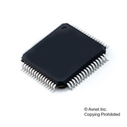
MCU 8-bit HCS08 CISC 64KB Flash 2.5V/3.3V 64-Pin LQFP Tray, MC9S08LH64CLH, NXP

Freescale"s S08 ultra-low-power MCU features a LCD driver and increased analog-to-digital converter (ADC) accuracy for medical and metering applications. The MC9S08LH family, with up to 64 KB flash, helps you reach target performance levels while minimizing power consumption in your design, demonstrating extreme energy efficiency for ultra-long operation in battery-powered applications.

  • 8-bit HCS08 Central Processor Unit (CPU)
  • Up to 40 MHz CPU at 3.6 V to 2.1 V across temperature range of –40 °C to 85 °C
  • Up to 20 MHz at 2.1 V to 1.8 V across temperature range of –40 °C to 85 °C
  • HC08 instruction set with added BGND instruction
  • Support for up to 32 interrupt/reset sources
  • On-Chip Memory
    • Dual array flash read/program/erase over full operating voltage and temperature
    • Random-access memory (RAM)
  • Security circuitry to prevent unauthorized access to RAM and flash contents
  • Power-Saving Modes
    • Two low-power stop modes
    • Reduced-power wait mode
      • Low-power run and wait modes allow peripherals to run while voltage regulator is in standby
      • Peripheral clock gating register can disable clocks to unused modules, thereby reducing currents
      • Very low-power external oscillator that can be used in stop2 or stop3 modes to provide accurate clock source to time-of-day (TOD) module
      • 6 µs typical wakeup time from stop3 mode
      • Clock Source Options
      • Oscillator (XOSC)
      • Loop-control Pierce oscillator; crystal or ceramic resonator range of 31.25 kHz to 38.4 kHz or 1 MHz to 16 MHz
      • Internal Clock Source (ICS)
      • Internal clock source module containing a frequency-locked-loop (FLL) controlled by internal or external reference; precision trimming of internal reference allows 0.2% resolution and 2% deviation over temperature and voltage; supporting bus frequencies from 1 MHz to 20 MHz
      • System Protection
      • Watchdog computer operating properly (COP) reset with option to run from dedicated 1 kHz internal clock source or bus clock
      • Low-voltage warning with interrupt
      • Low-voltage detection with reset or interrupt
      • Illegal opcode detection with reset; illegal address detection with reset
        • Flash block protection
        • Development Support
        • Single-wire background debug interface
      • LCD – Up to 8×36 or 4×40 LCD driver with internal charge pump and option to provide an internally-regulated LCD reference that can be trimmed for contrast control
      • ADC – 16-bit resolution; with a dedicated differential ADC input, and 8 single-ended ADC inputs; up to 2.5 µs conversion time; hardware averaging; calibration registers, automatic compare function; temperature sensor; operation in stop3; fully functional from 3.6 V to 1.8 V
      • IIC – Inter-integrated circuit bus module to operate at up to 100 kbps with maximum bus loading; multi-master operation; programmable slave address; interrupt-driven byte-by-byte data transfer; broadcast mode; 10-bit addressing
      • ACMP — Analog comparator with selectable interrupt on rising, falling, or either edge of comparator output; compare option to fixed internal reference voltage; outputs can be optionally routed to TPM module; operation in stop3
      • SCIx — Two full-duplex non-return to zero (NRZ) modules (SCI1 and SCI2); LIN master extended break generation; LIN slave extended break detection; wakeup on active edge
      • SPI — Full-duplex or single-wire bidirectional; double-buffered transmit and receive; master or slave mode; MSB-first or LSB-first shifting
      • TPMx — Two 2-channel (TPM1 and TPM2); selectable input capture, output compare, or buffered edge- or center-aligned PWM on each channel
Характеристики

Analog_comparators

3

On_chip_adc

8-chx16-bit

Max_operating_supply_voltage

3.6 V

Watchdog

1

Supplier_package

LQFP

Specifications

https://4donline.ihs.com/images/VipMasterIC/IC/FSCL/FSCLS07433/FSCLS07433-1.pdf?hkey=52A5661711E402568146F3353EA87419

Special_features

LCD Controller

Schedule_b

8542310000

Ram_size

4000 byte

Program_memory_type

Flash

Program_memory_size

64 KB

Product_dimensions

10 x 10 x 1.45 mm

Pin_count

64

Operating_temperature

-40 to 85 °C

Operating_supply_voltage

2.5, 3.3 V

Number_of_programmable_i_os

37

Бренд

Msl_level

3

Mounting

Surface Mount

Maximum_speed

40 MHz

Max_processing_temp

260

Lead_finish

Matte Tin

Lcd_segments

192, 112

Тип интерфейса

I2C/SCI/SPI

Instruction_set_architecture

CISC

Htsn

8542310001

Eccn

3A991.A.2

Data_bus_width

8 Bit

Country_of_origin

China

Min_operating_supply_voltage

1.8 V

Артикул: MC9S08LH64CLH

Описание

Freescale"s S08 ultra-low-power MCU features a LCD driver and increased analog-to-digital converter (ADC) accuracy for medical and metering applications. The MC9S08LH family, with up to 64 KB flash, helps you reach target performance levels while minimizing power consumption in your design, demonstrating extreme energy efficiency for ultra-long operation in battery-powered applications.

  • 8-bit HCS08 Central Processor Unit (CPU)
  • Up to 40 MHz CPU at 3.6 V to 2.1 V across temperature range of –40 °C to 85 °C
  • Up to 20 MHz at 2.1 V to 1.8 V across temperature range of –40 °C to 85 °C
  • HC08 instruction set with added BGND instruction
  • Support for up to 32 interrupt/reset sources
  • On-Chip Memory
    • Dual array flash read/program/erase over full operating voltage and temperature
    • Random-access memory (RAM)
  • Security circuitry to prevent unauthorized access to RAM and flash contents
  • Power-Saving Modes
    • Two low-power stop modes
    • Reduced-power wait mode
      • Low-power run and wait modes allow peripherals to run while voltage regulator is in standby
      • Peripheral clock gating register can disable clocks to unused modules, thereby reducing currents
      • Very low-power external oscillator that can be used in stop2 or stop3 modes to provide accurate clock source to time-of-day (TOD) module
      • 6 µs typical wakeup time from stop3 mode
      • Clock Source Options
      • Oscillator (XOSC)
      • Loop-control Pierce oscillator; crystal or ceramic resonator range of 31.25 kHz to 38.4 kHz or 1 MHz to 16 MHz
      • Internal Clock Source (ICS)
      • Internal clock source module containing a frequency-locked-loop (FLL) controlled by internal or external reference; precision trimming of internal reference allows 0.2% resolution and 2% deviation over temperature and voltage; supporting bus frequencies from 1 MHz to 20 MHz
      • System Protection
      • Watchdog computer operating properly (COP) reset with option to run from dedicated 1 kHz internal clock source or bus clock
      • Low-voltage warning with interrupt
      • Low-voltage detection with reset or interrupt
      • Illegal opcode detection with reset; illegal address detection with reset
        • Flash block protection
        • Development Support
        • Single-wire background debug interface
      • LCD – Up to 8×36 or 4×40 LCD driver with internal charge pump and option to provide an internally-regulated LCD reference that can be trimmed for contrast control
      • ADC – 16-bit resolution; with a dedicated differential ADC input, and 8 single-ended ADC inputs; up to 2.5 µs conversion time; hardware averaging; calibration registers, automatic compare function; temperature sensor; operation in stop3; fully functional from 3.6 V to 1.8 V
      • IIC – Inter-integrated circuit bus module to operate at up to 100 kbps with maximum bus loading; multi-master operation; programmable slave address; interrupt-driven byte-by-byte data transfer; broadcast mode; 10-bit addressing
      • ACMP — Analog comparator with selectable interrupt on rising, falling, or either edge of comparator output; compare option to fixed internal reference voltage; outputs can be optionally routed to TPM module; operation in stop3
      • SCIx — Two full-duplex non-return to zero (NRZ) modules (SCI1 and SCI2); LIN master extended break generation; LIN slave extended break detection; wakeup on active edge
      • SPI — Full-duplex or single-wire bidirectional; double-buffered transmit and receive; master or slave mode; MSB-first or LSB-first shifting
      • TPMx — Two 2-channel (TPM1 and TPM2); selectable input capture, output compare, or buffered edge- or center-aligned PWM on each channel
Детали

Analog_comparators

3

On_chip_adc

8-chx16-bit

Max_operating_supply_voltage

3.6 V

Watchdog

1

Supplier_package

LQFP

Specifications

https://4donline.ihs.com/images/VipMasterIC/IC/FSCL/FSCLS07433/FSCLS07433-1.pdf?hkey=52A5661711E402568146F3353EA87419

Special_features

LCD Controller

Schedule_b

8542310000

Ram_size

4000 byte

Program_memory_type

Flash

Program_memory_size

64 KB

Product_dimensions

10 x 10 x 1.45 mm

Pin_count

64

Operating_temperature

-40 to 85 °C

Operating_supply_voltage

2.5, 3.3 V

Number_of_programmable_i_os

37

Бренд

Msl_level

3

Mounting

Surface Mount

Maximum_speed

40 MHz

Max_processing_temp

260

Lead_finish

Matte Tin

Lcd_segments

192, 112

Тип интерфейса

I2C/SCI/SPI

Instruction_set_architecture

CISC

Htsn

8542310001

Eccn

3A991.A.2

Data_bus_width

8 Bit

Country_of_origin

China

Min_operating_supply_voltage

1.8 V