MCU 8-bit HC08 CISC 4KB Flash 3.3V/5V 28-Pin PDIP Rail, MC908GR4CPE, NXP

The MC68HC908GR4 is a device identical to the MC68HC908GR8 except that it has less Flash memory. Only when the MC68HC908GR4 specifically mentioned in the text.

  • High-performance M68HC08 architecture optimized for C-compilers
  • Fully upward-compatible object code with M6805, M146805, and M68HC05 Families
  • 8-MHz internal bus frequency
  • FLASH program memory security(1)
  • On-chip programming firmware for use with host personal computer which does not require high voltage for entry
  • In-system programming
  • System protection features:
    • Optional computer operating properly (COP) reset
    • Low-voltage detection with optional reset and selectable trip points for 3.0 V and 5.0 V operation
    • Illegal opcode detection with reset
    • Illegal address detection with reset
  • Low-power design; fully static with stop and wait modes
  • Standard low-power modes of operation: -Wait mode
    • Stop mode
  • Master reset pin and power-on reset (POR)
  • The MC68HC908GR4 with in-circuit programming capabilities of FLASH program memory
  • 384 bytes of on-chip random-access memory (RAM)
  • Serial peripheral interface module (SPI)
  • Serial communications interface module (SCI)
  • One 16-bit, 2-channel timer (TIM1) and one 16-bit, 1-channel timer (TIM2) interface modules with selectable input capture, output compare, and PWM capability on each channel
  • 6-channel, 8-bit successive approximation analog-to-digital converter (ADC)
  • BREAK module (BRK) to allow single breakpoint setting during in-circuit debugging
  • Internal pullups on IRQ and RST to reduce customer system cost
  • Clock generator module with on-chip 32-kHz crystal compatible PLL (phase-lock loop)
  • Up to 21 general-purpose input/output (I/O) pins, including:
    • 19 shared-function I/O pins
    • Up to two dedicated I/O pins, depending on package choice
  • Selectable pullups on inputs only on ports A, C, and D. Selection is on an individual port bit basis. During output mode, pullups are disengaged.
  • High current 10-mA sink/10-mA source capability on all port pins
  • Higher current 15-mA sink/source capability on PTC0–PTC1
  • Timebase module with clock prescaler circuitry for eight user selectable periodic real-time interrupts with optional active clock source during stop mode for periodic wakeup from stop using an external 32-kHz crystal
  • Oscillator stop mode enable bit (OSCSTOPENB) in the CONFIG register to allow user selection of having the oscillator enabled or disabled during stop mode
  • 4-bit keyboard wakeup port
  • 42-pin shrink dual in-line package (SDIP), 32-pin quad flat pack (QFP), 28-pin plastic dual-in-line package (DIP), or 28-pin small outline integrated circuit (SOIC)
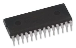
Характеристики

Бренд

Operating_temperature

-40 to 85 °C

Min_operating_supply_voltage

2.7 V

Max_operating_supply_voltage

5.5 V

Supplier_package

PDIP

Specifications

http://cache.freescale.com/files/microcontrollers/doc/data_sheet/MC68HC908GR8.pdf

Schedule_b

8542390000

Ram_size

384 byte

Program_memory_type

Flash

Program_memory_size

4 Kb

Product_dimensions

37.21 x 14.22 x 4.06 mm

Pin_count

28

Operating_supply_voltage

3.3, 5 V

Country_of_origin

United States

On_chip_adc

6-chx8-bit

Number_of_timers

3

Number_of_programmable_i_os

21

Mounting

Through Hole

Maximum_speed

8.2 MHz

Lead_finish

Matte Tin

Тип интерфейса

SCI/SPI

Instruction_set_architecture

CISC

Htsn

8542310001

Eccn

EAR99

Data_bus_width

8 Bit

Max_expanded_memory_size

64 KB

Артикул: MC908GR4CPE

Описание

The MC68HC908GR4 is a device identical to the MC68HC908GR8 except that it has less Flash memory. Only when the MC68HC908GR4 specifically mentioned in the text.

  • High-performance M68HC08 architecture optimized for C-compilers
  • Fully upward-compatible object code with M6805, M146805, and M68HC05 Families
  • 8-MHz internal bus frequency
  • FLASH program memory security(1)
  • On-chip programming firmware for use with host personal computer which does not require high voltage for entry
  • In-system programming
  • System protection features:
    • Optional computer operating properly (COP) reset
    • Low-voltage detection with optional reset and selectable trip points for 3.0 V and 5.0 V operation
    • Illegal opcode detection with reset
    • Illegal address detection with reset
  • Low-power design; fully static with stop and wait modes
  • Standard low-power modes of operation: -Wait mode
    • Stop mode
  • Master reset pin and power-on reset (POR)
  • The MC68HC908GR4 with in-circuit programming capabilities of FLASH program memory
  • 384 bytes of on-chip random-access memory (RAM)
  • Serial peripheral interface module (SPI)
  • Serial communications interface module (SCI)
  • One 16-bit, 2-channel timer (TIM1) and one 16-bit, 1-channel timer (TIM2) interface modules with selectable input capture, output compare, and PWM capability on each channel
  • 6-channel, 8-bit successive approximation analog-to-digital converter (ADC)
  • BREAK module (BRK) to allow single breakpoint setting during in-circuit debugging
  • Internal pullups on IRQ and RST to reduce customer system cost
  • Clock generator module with on-chip 32-kHz crystal compatible PLL (phase-lock loop)
  • Up to 21 general-purpose input/output (I/O) pins, including:
    • 19 shared-function I/O pins
    • Up to two dedicated I/O pins, depending on package choice
  • Selectable pullups on inputs only on ports A, C, and D. Selection is on an individual port bit basis. During output mode, pullups are disengaged.
  • High current 10-mA sink/10-mA source capability on all port pins
  • Higher current 15-mA sink/source capability on PTC0–PTC1
  • Timebase module with clock prescaler circuitry for eight user selectable periodic real-time interrupts with optional active clock source during stop mode for periodic wakeup from stop using an external 32-kHz crystal
  • Oscillator stop mode enable bit (OSCSTOPENB) in the CONFIG register to allow user selection of having the oscillator enabled or disabled during stop mode
  • 4-bit keyboard wakeup port
  • 42-pin shrink dual in-line package (SDIP), 32-pin quad flat pack (QFP), 28-pin plastic dual-in-line package (DIP), or 28-pin small outline integrated circuit (SOIC)

Детали

Бренд

Operating_temperature

-40 to 85 °C

Min_operating_supply_voltage

2.7 V

Max_operating_supply_voltage

5.5 V

Supplier_package

PDIP

Specifications

http://cache.freescale.com/files/microcontrollers/doc/data_sheet/MC68HC908GR8.pdf

Schedule_b

8542390000

Ram_size

384 byte

Program_memory_type

Flash

Program_memory_size

4 Kb

Product_dimensions

37.21 x 14.22 x 4.06 mm

Pin_count

28

Operating_supply_voltage

3.3, 5 V

Country_of_origin

United States

On_chip_adc

6-chx8-bit

Number_of_timers

3

Number_of_programmable_i_os

21

Mounting

Through Hole

Maximum_speed

8.2 MHz

Lead_finish

Matte Tin

Тип интерфейса

SCI/SPI

Instruction_set_architecture

CISC

Htsn

8542310001

Eccn

EAR99

Data_bus_width

8 Bit

Max_expanded_memory_size

64 KB