Описание
The AVR core combines a rich instruction set with 32 general purpose working registers. All 32 registers are directly connected to the Arithmetic Logic Unit (ALU), allowing two independent registers to be accessed in one single instruction executed in one clock cycle. The resulting architecture is more code efficient while achieving throughputs up to ten times faster than conventional CISC microcontrollers. The ATtiny24/44/84 provides the following features: 2/4/8K byte of In-System Programmable Flash, 128/256/512 bytes EEPROM, 128/256/512 bytes SRAM, 12 general purpose I/O lines, 32 general purpose working registers, an 8-bit Timer/Counter with two PWM channels, a 16-bit timer/counter with two PWM channels, Internal and External Interrupts, a 8-channel 10-bit ADC, programmable gain stage (1x, 20x) for 12 differential ADC channel pairs, a programmable Watchdog Timer with internal oscillator, internal calibrated oscillator, and four software selectable power saving modes. Idle mode stops the CPU while allowing the SRAM, Timer/Counter, ADC, Analog Comparator, and Interrupt system to continue functioning. ADC Noise Reduction mode minimizes switching noise during ADC conversions by stopping the CPU and all I/O modules except the ADC. In Power-down mode registers keep their contents and all chip functions are disbaled until the next interrupt or hardware reset. In Standby mode, the crystal/resonator oscillator is running while the rest of the device is sleeping, allowing very fast start-up combined with low power consumption. The device is manufactured using Microchip’s high density non-volatile memory technology. The onchip ISP Flash allows the Program memory to be re-programmed in-system through an SPI serial interface, by a conventional non-volatile memory programmer or by an on-chip boot code running on the AVR core. The ATtiny24/44/84 AVR is supported with a full suite of program and system development tools including: C Compilers, Macro Assemblers, Program Debugger/Simulators and Evaluation kits.
- High Performance, Low Power AVR® 8-Bit Microcontroller
- Advanced RISC Architecture
- 120 Powerful Instructions –Most Single Clock Cycle Execution
- 32 x 8 General Purpose Working Registers
- Fully Static Operation
- Non-Volatile Program and Data Memories
- 2/4/8K Bytes of In-System Programmable Program Memory Flash
- Endurance: 10,000 Write/Erase Cycles
- 128/256/512 Bytes of In-System Programmable EEPROM
- Endurance: 100,000 Write/Erase Cycles
- 128/256/512 Bytes of Internal SRAM
- Data Retention: 20 years at 85°C / 100 years at 25°C
- Programming Lock for Self-Programming Flash & EEPROM Data Security
- Peripheral Features
- One 8-Bit and One 16-Bit Timer/Counter with Two PWM Channels, Each
- 10-bit ADC
- 8 Single-Ended Channels
- 12 Differential ADC Channel Pairs with Programmable Gain (1x / 20x)
- Programmable Watchdog Timer with Separate On-chip Oscillator
- On-chip Analog Comparator
- Universal Serial Interface
- Special Microcontroller Features
- debugWIRE On-chip Debug System
- In-System Programmable via SPI Port
- Internal and External Interrupt Sources: Pin Change Interrupt on 12 Pins
- Low Power Idle, ADC Noise Reduction, Standby and Power-Down Modes
- Enhanced Power-on Reset Circuit
- Programmable Brown-out Detection Circuit
- Internal Calibrated Oscillator
- On-chip Temperature Sensor
- I/O and Packages
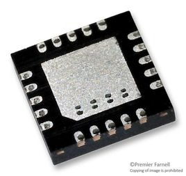
- Available in 20-Pin QFN/MLF & 14-Pin SOIC and PDIP
- Twelve Programmable I/O Lines
- Operating Voltage:2.7 –5.5V
- Speed Grade
- ATtiny24V/44V/84V
- 0 –4 MH–@ 1.8 –5.5V
- 0 –10 MH–@ 2.7 –5.5V
- ATtiny24/44/84
- 0 –10 MH–@ 2.7 –5.5V
- 0 –20 MH–@ 4.5 –5.5V
- Industrial Temperature Range: -40°C to +85°C
- Low Power Consumption
- Active Mode (1 MH–System Clock): 300 µA @ 1.8V
- Power-Down Mode: 0.1 µA @ 1.8V


