Описание
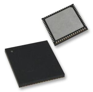
The ATmega256RFR2 is a low-power CMOS 8-bit microcontroller based on the AVR enhanced RISC architecture combined with a high data rate transceiver for the 2.4 GHz ISM band. By executing powerful instructions in a single clock cycle, the device achieves throughputs approaching 1 MIPS per MHz allowing the system designer to optimize power consumption versus processing speed. The radio transceiver provides high data rates from 250 kb/s up to 2 Mb/s, frame handling, outstanding receiver sensitivity and high transmit output power enabling a very robust wireless communication. The AVR core combines a rich instruction set with 32 general purpose working registers. All 32 registers are directly connected to the Arithmetic Logic Unit (ALU). Two independent registers can be accessed with one single instruction executed in one clock cycle. The resulting architecture is very code efficient while achieving throughputs up to ten times faster than conventional CISC microcontrollers. The system includes internal voltage regulation and an advanced power management. Distinguished by the small leakage current it allows an extended operation time from battery.
- Network support by hardware assisted Multiple PAN Address Filtering
- Advanced Hardware assisted Reduced Power Consumption
- High Performance, Low Power AVR®
- 8
- Bit Microcontroller
- Advanced RISC Architecture
- 135 Powerful Instructions – Most Single Clock Cycle Execution
- 32×8 General Purpose Working Registers / On Chip 2
- cycle Multiplier
- Up to 16 MIPS Throughput at 16 MHz and 1.8V – Fully Static Operation
- Nonvolatile Program and Data Memories
- 256K Bytes of In System Self Programmable Flash
- Endurance: 10’000 Write/Erase Cycles @ 125°C (25’000 Cycles @ 85°C)
- 8K Bytes EEPROM
- Endurance: 20’000 Write/Erase Cycles @ 125°C (100’000 Cycles @ 25°C)
- 32K Bytes Internal SRAM
- JTAG (IEEE std. 1149.1 compliant) Interface
- Boundary scan Capabilities According to the JTAG Standard
- Extensive On chip Debug Support
- Programming of Flash EEPROM, Fuses and Lock Bits through the JTAG interface
- Peripheral Features
- Multiple Timer/Counter & PWM channels
- Real Time Counter with Separate Oscillator
- 10
- bit, 330 ks/s A/D Converter; Analog Comparator; On chip Temperature Sensor
- Master/Slave SPI Serial Interface
- Two Programmable Serial USART
- Byte Oriented 2
- wire Serial Interface
- Advanced Interrupt Handler and Power Save Modes
- Watchdog Timer with Separate On Chip Oscillator
- Power on Reset and Low Current Brownout Detector
- Fully integrated Low Power Transceiver for 2.4 GHz ISM Band
- High Power Amplifier support by TX spectrum side lobe suppression
- Supported Data Rates: 250 kb/s and 500 kb/s, 1 Mb/s, 2 Mb/s
- 100 dBm RX Sensitivity; TX Output Power up to 3.5 dBm
- Hardware Assisted MAC (Auto Acknowledge, Auto Retry)
- 32 Bit IEEE 802.15.4 Symbol Counter
- SFD
- Detection, Spreading; Dispreading; Framing ; CRC
- 16 Computation
- Antenna Diversity and TX/RX control / TX/RX 128 Byte Frame Buffer
- Phase measurement support
- PLL synthesizer with 5 MHz and 500 kHz channel spacing for 2.4 GHz ISM Band
- Hardware Security (AES, True Random Generator)
- Integrated Crystal Oscillators (32.768 kHz & 16 MHz, external crystal needed)
- I/O and Package
- 38 Programmable I/O Lines
- 64
- pad QFN (RoHS/Fully Green)
- Temperature Range:
- 40°C to 125°C Industrial
- Ultra Low Power consumption (1.8 to 3.6V) for AVR & Rx/Tx: 10.1mA/18.6 am
- CPU Active Mode (16MHz): 4.1 am
- 2.4GHz Transceiver: RX_ON 6.0 am / TX 14.5 am (maximum TX output power)
- Deep Sleep Mode: <700nA @ 25°C
- Speed Grade: 0 – 16 MHz @ 1.8 – 3.6V range with integrated voltage regulators


