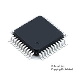
MCU 8-bit AT89 80C51 CISC 4KB Flash 2.5V/3.3V/5V 44-Pin TQFP, AT89LP51-20AU, Microchip

The AT89LP51 is a low-power, high-performance CMOS 8-bit microcontroller with 4K bytes of In-System Programmable Flash program memory and 256 bytes of Flash data memory. The device is manufactured using "s high-density nonvolatile memory technology and is compatible with the industry-standard 80C52 instruction set. The89LP51 is built around an enhanced CPU core that can fetch a single byte from memory every clock cycle. In the classic 8051 architecture, each fetch requires 6 clock cycles, forcing instructions to execute in 12, 24 or 48 clock cycles. In the AT89LP51 CPU, instructions need only 1 to 4 clock cycles providing 6 to 12 times more throughput than the standard 8051. Seventy percent of instructions need only as many clock cycles as they have bytes to execute, and most of the remaining instructions require only one additional clock. The enhanced CPU core is capable of 20 MIPS throughput whereas the classic 8051 CPU can deliver only 4 MIPS at the same current consumption. Conversely, at the same throughput as the classic 8051, the new CPU core runs at a much lower speed and thereby greatly reducing power consumption and EMI. The AT89LP51 also includes a compatibility mode that will enable classic 12 clock per machine cycle operation for true timing compatibility with AT89S51 The AT89LP51 provides the following standard features: 4K/8K bytes of In-System Programmable Flash program memory, 256 bytes of Flash data memory, 256 bytes of RAM, up to 36 I/O lines, three 16-bit timer/counters, a programmable watchdog timer, a full-duplex serial port, an on-chip crystal oscillator, an internal 1.8432 MHz auxiliary oscillator, and a four-level, six-vector interrupt system.

  • 8-bit Microcontroller Compatible with 8051 Products
  • Enhanced 8051 Architecture
    • Single Clock Cycle per Byte Fetch
    • 12 Clock per Machine Cycle Compatibility Mode
    • Up to 20 MIPS Throughput at 20 MHz Clock Frequency
    • Fully Static Operation: 0 Hz to 20 MHz
    • On-chip 2-cycle Hardware Multiplier
    • 256 x 8 Internal RAM
    • External Data/Program Memory Interface
    • Dual Data Pointers
    • 4-level Interrupt Priority
  • Nonvolatile Program and Data Memory
    • 4K/8K Bytes of In-System Programmable (ISP) Flash Program Memory
    • 256 Bytes of Flash Data Memory
    • 256-byte User Signature Array
    • Endurance: 10,000 Write/Erase Cycles
    • Serial Interface for Program Downloading
    • 64-byte Fast Programming Mode
    • 3-level Program Memory Lock for Software Security
    • In-Application Programming of Program Memory
  • Special Microcontroller Features
    • Brown-out Detection and Power-on Reset with Power-off Flag
    • Selectable Polarity External Reset Pin
    • Low Power Idle and Power-down Modes
    • Interrupt Recovery from Power-down Mode
    • Internal 1.8432 MHz Auxiliary Oscillator
  • Operating Conditions
    • 2.4V to 5.5V VCC Voltage Range
    • -40°C to 85°C Temperature Range
    • 0 to 20 MHz @ 2.4V–5.5V
    • 0 to 25 MHz @ 4.5V–5.5V

Характеристики

Бренд

Number_of_timers

3

Max_operating_supply_voltage

5.5 V

Watchdog

1

Supplier_package

TQFP

Specifications

https://4donline.ihs.com/images/VipMasterIC/IC/ATML/ATMLS06221/ATMLS06221-1.pdf?hkey=52A5661711E402568146F3353EA87419

Screening_level

Industrial

Schedule_b

8542390000

Ram_size

256 byte

Program_memory_type

Flash

Program_memory_size

4 Kb

Product_dimensions

10.1 x 10.1 x 1.05 mm

Pin_count

44

Operating_temperature

-40 to 85 °C

Operating_supply_voltage

2.5, 3.3, 5 V

Number_of_programmable_i_os

36

Country_of_origin

China

Msl_level

3

Mounting

Surface Mount

Maximum_speed

20 MHz

Max_processing_temp

260

Lead_finish

Matte Tin

Тип интерфейса

UART

Instruction_set_architecture

CISC

Htsn

8542310001

Eccn

EAR99

Device_core

80C51

Data_memory_size

256 byte

Data_bus_width

8 Bit

Min_operating_supply_voltage

2.4 V

Артикул: AT89LP51-20AU

Описание

The AT89LP51 is a low-power, high-performance CMOS 8-bit microcontroller with 4K bytes of In-System Programmable Flash program memory and 256 bytes of Flash data memory. The device is manufactured using "s high-density nonvolatile memory technology and is compatible with the industry-standard 80C52 instruction set. The89LP51 is built around an enhanced CPU core that can fetch a single byte from memory every clock cycle. In the classic 8051 architecture, each fetch requires 6 clock cycles, forcing instructions to execute in 12, 24 or 48 clock cycles. In the AT89LP51 CPU, instructions need only 1 to 4 clock cycles providing 6 to 12 times more throughput than the standard 8051. Seventy percent of instructions need only as many clock cycles as they have bytes to execute, and most of the remaining instructions require only one additional clock. The enhanced CPU core is capable of 20 MIPS throughput whereas the classic 8051 CPU can deliver only 4 MIPS at the same current consumption. Conversely, at the same throughput as the classic 8051, the new CPU core runs at a much lower speed and thereby greatly reducing power consumption and EMI. The AT89LP51 also includes a compatibility mode that will enable classic 12 clock per machine cycle operation for true timing compatibility with AT89S51 The AT89LP51 provides the following standard features: 4K/8K bytes of In-System Programmable Flash program memory, 256 bytes of Flash data memory, 256 bytes of RAM, up to 36 I/O lines, three 16-bit timer/counters, a programmable watchdog timer, a full-duplex serial port, an on-chip crystal oscillator, an internal 1.8432 MHz auxiliary oscillator, and a four-level, six-vector interrupt system.

  • 8-bit Microcontroller Compatible with 8051 Products
  • Enhanced 8051 Architecture
    • Single Clock Cycle per Byte Fetch
    • 12 Clock per Machine Cycle Compatibility Mode
    • Up to 20 MIPS Throughput at 20 MHz Clock Frequency
    • Fully Static Operation: 0 Hz to 20 MHz
    • On-chip 2-cycle Hardware Multiplier
    • 256 x 8 Internal RAM
    • External Data/Program Memory Interface
    • Dual Data Pointers
    • 4-level Interrupt Priority
  • Nonvolatile Program and Data Memory
    • 4K/8K Bytes of In-System Programmable (ISP) Flash Program Memory
    • 256 Bytes of Flash Data Memory
    • 256-byte User Signature Array
    • Endurance: 10,000 Write/Erase Cycles
    • Serial Interface for Program Downloading
    • 64-byte Fast Programming Mode
    • 3-level Program Memory Lock for Software Security
    • In-Application Programming of Program Memory
  • Special Microcontroller Features
    • Brown-out Detection and Power-on Reset with Power-off Flag
    • Selectable Polarity External Reset Pin
    • Low Power Idle and Power-down Modes
    • Interrupt Recovery from Power-down Mode
    • Internal 1.8432 MHz Auxiliary Oscillator
  • Operating Conditions
    • 2.4V to 5.5V VCC Voltage Range
    • -40°C to 85°C Temperature Range
    • 0 to 20 MHz @ 2.4V–5.5V
    • 0 to 25 MHz @ 4.5V–5.5V

Детали

Бренд

Number_of_timers

3

Max_operating_supply_voltage

5.5 V

Watchdog

1

Supplier_package

TQFP

Specifications

https://4donline.ihs.com/images/VipMasterIC/IC/ATML/ATMLS06221/ATMLS06221-1.pdf?hkey=52A5661711E402568146F3353EA87419

Screening_level

Industrial

Schedule_b

8542390000

Ram_size

256 byte

Program_memory_type

Flash

Program_memory_size

4 Kb

Product_dimensions

10.1 x 10.1 x 1.05 mm

Pin_count

44

Operating_temperature

-40 to 85 °C

Operating_supply_voltage

2.5, 3.3, 5 V

Number_of_programmable_i_os

36

Country_of_origin

China

Msl_level

3

Mounting

Surface Mount

Maximum_speed

20 MHz

Max_processing_temp

260

Lead_finish

Matte Tin

Тип интерфейса

UART

Instruction_set_architecture

CISC

Htsn

8542310001

Eccn

EAR99

Device_core

80C51

Data_memory_size

256 byte

Data_bus_width

8 Bit

Min_operating_supply_voltage

2.4 V