MCU 8-Bit 8FX F2MC-8FX CISC 36KB Flash 2.5V/3.3V/5V 24-Pin TSSOP, MB95F656EPFT-G-SNE2, Rochester Electronics

The MB95F656E is a series of general-purpose, single-chip microcontrollers. In addition to a compact instruction set, the microcontrollers of this series contain a variety of peripheral functions

  • F2MC-8FX CPU core Instruction set optimized for controllers
  • Multiplication and division instructions
  • 16-bit arithmetic operations
  • Bit test branch instructions
  • Bit manipulation instructions, etc. Note: F2MC is the abbreviation of FUJITSU Flexible Microcontroller.
  • Clock
  • Selectable main clock source
    • Main oscillation clock (up to 16.25 MHz, maximum machine clock frequency: 8.125 MHz)
    • External clock (up to 32.5 MHz, maximum machine clock frequency: 16.25 MHz)
    • Main CR clock (4 MHz ±2%)
    • Main CR PLL clock
    • The main CR PLL clock frequency becomes 8 MHz ±2% when the PLL multiplication rate is 2.
    • The main CR PLL clock frequency becomes 10 MHz ±2% when the PLL multiplication rate is 2.5.
    • The main CR PLL clock frequency becomes 12 MHz ±2% when the PLL multiplication rate is 3.
    • The main CR PLL clock frequency becomes 16 MHz ±2% when the PLL multiplication rate is 4.
    • Main PLL clock (maximum machine clock frequency: 16 MHz)
  • Selectable subclock source
    • Suboscillation clock (32.768 kHz)
    • External clock (32.768 kHz)
    • Sub-CR clock (Typ: 100 kHz, Min: 50 kHz, Max: 150 kHz)
  • Timer
  • 8/16-bit composite timer × 2 channels
  • Time-base timer × 1 channel
  • Watch prescaler × 1 channel
  • UART/SIO × 1 channel (The channel can be used either as a UART/SIO channel or as an I2C bus interface channel.)
  • The function of this channel can be switched between UART/SIO and I2C bus interface.
  • Full duplex double buffer
  • Capable of clock asynchronous (UART) serial data transfer and clock synchronous (SIO) serial data transfer
  • I2C bus interface × 2 channels (One of the two channels can be used either as an I2C bus interface channel or as a UART/SIO channel.)
  • Supports Standard-mode and Fast-mode (400 kHz).
  • Built-in wake-up function
  • LIN-UART
  • Full duplex double buffer
  • Capable of clock asynchronous serial data transfer and clock synchronous serial data transfer
  • External interrupt × 6 channels
  • Interrupt by edge detection (rising edge, falling edge, and both edges can be selected)
  • Can be used to wake up the device from different low power consumption (standby) modes
  • 8/12-bit A/D converter × 6 channels 8-bit or 12-bit resolution can be selected.
  • Low power consumption (standby) modes There are four standby modes as follows:
  • Stop mode
  • Sleep mode
  • Watch mode
  • Time-base timer mode
  • I/O port
  • MB95F652E/F653E/F654E/F656E (number of I/O ports: 21)
    • General-purpose I/O ports (CMOS I/O) : 17
    • General-purpose I/O ports (N-ch open drain) : 4
  • MB95F652L/F653L/F654L/F656L (number of I/O ports: 20)
    • General-purpose I/O ports (CMOS I/O) : 17
    • General-purpose I/O ports (N-ch open drain) : 3
  • On-chip debug
  • 1-wire serial control
  • Serial writing supported (asynchronous mode)
  • Hardware/software watchdog timer
  • Built-in hardware watchdog timer
  • Built-in software watchdog timer
  • Power-on reset A power-on reset is generated when the power is switched on Built-in low-voltage detection function
  • Clock supervisor counter Built-in clock supervisor counter
  • Dual operation Flash memory The program/erase operation and the read operation can be executed in different banks (upper bank/lower bank) simultaneously.
  • Flash memory security function Protects the content of the Flash memory
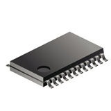
Характеристики

Бренд

Country_of_origin

United States

Data_bus_width

8 Bit

Device_core

F2MC-8FX

Eccn

3A991.A

Htsn

8542310001

Instruction_set_architecture

CISC

Тип интерфейса

I2C/LIN/SIO/UART

Maximum_speed

16.25 MHz

Mounting

Surface Mount

Number_of_programmable_i_os

21

Number_of_timers

3

On_chip_adc

6-chx8/12-bit

Operating_supply_voltage

2.5, 3.3, 5 V

Operating_temperature

-40 to 85 °C

Pin_count

24

Product_dimensions

7.8 x 4.4 x 1.1(Max)

Program_memory_size

36 KB

Program_memory_type

Flash

Ram_size

1 KB

Schedule_b

8542390000

Screening_level

Industrial

Specifications

https://4donline.ihs.com/images/VipMasterIC/IC/CYPR/CYPR-S-A0006313869/CYPR-S-A0006313854-1.pdf?hkey=52A5661711E402568146F3353EA87419

Supplier_package

TSSOP

Watchdog

2

Max_operating_supply_voltage

5.5 V

Min_operating_supply_voltage

1.8 V

Max_expanded_memory_size

64 KB

Артикул: MB95F656EPFT-G-SNE2

Описание

The MB95F656E is a series of general-purpose, single-chip microcontrollers. In addition to a compact instruction set, the microcontrollers of this series contain a variety of peripheral functions

  • F2MC-8FX CPU core Instruction set optimized for controllers
  • Multiplication and division instructions
  • 16-bit arithmetic operations
  • Bit test branch instructions
  • Bit manipulation instructions, etc. Note: F2MC is the abbreviation of FUJITSU Flexible Microcontroller.
  • Clock
  • Selectable main clock source
    • Main oscillation clock (up to 16.25 MHz, maximum machine clock frequency: 8.125 MHz)
    • External clock (up to 32.5 MHz, maximum machine clock frequency: 16.25 MHz)
    • Main CR clock (4 MHz ±2%)
    • Main CR PLL clock
    • The main CR PLL clock frequency becomes 8 MHz ±2% when the PLL multiplication rate is 2.
    • The main CR PLL clock frequency becomes 10 MHz ±2% when the PLL multiplication rate is 2.5.
    • The main CR PLL clock frequency becomes 12 MHz ±2% when the PLL multiplication rate is 3.
    • The main CR PLL clock frequency becomes 16 MHz ±2% when the PLL multiplication rate is 4.
    • Main PLL clock (maximum machine clock frequency: 16 MHz)
  • Selectable subclock source
    • Suboscillation clock (32.768 kHz)
    • External clock (32.768 kHz)
    • Sub-CR clock (Typ: 100 kHz, Min: 50 kHz, Max: 150 kHz)
  • Timer
  • 8/16-bit composite timer × 2 channels
  • Time-base timer × 1 channel
  • Watch prescaler × 1 channel
  • UART/SIO × 1 channel (The channel can be used either as a UART/SIO channel or as an I2C bus interface channel.)
  • The function of this channel can be switched between UART/SIO and I2C bus interface.
  • Full duplex double buffer
  • Capable of clock asynchronous (UART) serial data transfer and clock synchronous (SIO) serial data transfer
  • I2C bus interface × 2 channels (One of the two channels can be used either as an I2C bus interface channel or as a UART/SIO channel.)
  • Supports Standard-mode and Fast-mode (400 kHz).
  • Built-in wake-up function
  • LIN-UART
  • Full duplex double buffer
  • Capable of clock asynchronous serial data transfer and clock synchronous serial data transfer
  • External interrupt × 6 channels
  • Interrupt by edge detection (rising edge, falling edge, and both edges can be selected)
  • Can be used to wake up the device from different low power consumption (standby) modes
  • 8/12-bit A/D converter × 6 channels 8-bit or 12-bit resolution can be selected.
  • Low power consumption (standby) modes There are four standby modes as follows:
  • Stop mode
  • Sleep mode
  • Watch mode
  • Time-base timer mode
  • I/O port
  • MB95F652E/F653E/F654E/F656E (number of I/O ports: 21)
    • General-purpose I/O ports (CMOS I/O) : 17
    • General-purpose I/O ports (N-ch open drain) : 4
  • MB95F652L/F653L/F654L/F656L (number of I/O ports: 20)
    • General-purpose I/O ports (CMOS I/O) : 17
    • General-purpose I/O ports (N-ch open drain) : 3
  • On-chip debug
  • 1-wire serial control
  • Serial writing supported (asynchronous mode)
  • Hardware/software watchdog timer
  • Built-in hardware watchdog timer
  • Built-in software watchdog timer
  • Power-on reset A power-on reset is generated when the power is switched on Built-in low-voltage detection function
  • Clock supervisor counter Built-in clock supervisor counter
  • Dual operation Flash memory The program/erase operation and the read operation can be executed in different banks (upper bank/lower bank) simultaneously.
  • Flash memory security function Protects the content of the Flash memory
Детали

Бренд

Country_of_origin

United States

Data_bus_width

8 Bit

Device_core

F2MC-8FX

Eccn

3A991.A

Htsn

8542310001

Instruction_set_architecture

CISC

Тип интерфейса

I2C/LIN/SIO/UART

Maximum_speed

16.25 MHz

Mounting

Surface Mount

Number_of_programmable_i_os

21

Number_of_timers

3

On_chip_adc

6-chx8/12-bit

Operating_supply_voltage

2.5, 3.3, 5 V

Operating_temperature

-40 to 85 °C

Pin_count

24

Product_dimensions

7.8 x 4.4 x 1.1(Max)

Program_memory_size

36 KB

Program_memory_type

Flash

Ram_size

1 KB

Schedule_b

8542390000

Screening_level

Industrial

Specifications

https://4donline.ihs.com/images/VipMasterIC/IC/CYPR/CYPR-S-A0006313869/CYPR-S-A0006313854-1.pdf?hkey=52A5661711E402568146F3353EA87419

Supplier_package

TSSOP

Watchdog

2

Max_operating_supply_voltage

5.5 V

Min_operating_supply_voltage

1.8 V

Max_expanded_memory_size

64 KB